- 您现在的位置:买卖IC网 > PDF目录17079 > EVAL-AD5421SDZ (Analog Devices Inc)BOARD EVAL FOR AD5421 PDF资料下载
参数资料
| 型号: | EVAL-AD5421SDZ |
| 厂商: | Analog Devices Inc |
| 文件页数: | 4/36页 |
| 文件大小: | 0K |
| 描述: | BOARD EVAL FOR AD5421 |
| 标准包装: | 1 |
| DAC 的数量: | 1 |
| 位数: | 16 |
| 数据接口: | 串行,SPI? |
| 设置时间: | 50µs |
| DAC 型: | 电压 |
| 工作温度: | -40°C ~ 105°C |
| 已供物品: | 板 |
| 已用 IC / 零件: | AD5421 |
第1页第2页第3页当前第4页第5页第6页第7页第8页第9页第10页第11页第12页第13页第14页第15页第16页第17页第18页第19页第20页第21页第22页第23页第24页第25页第26页第27页第28页第29页第30页第31页第32页第33页第34页第35页第36页
AD5421
Data Sheet
Rev. G | Page 12 of 36
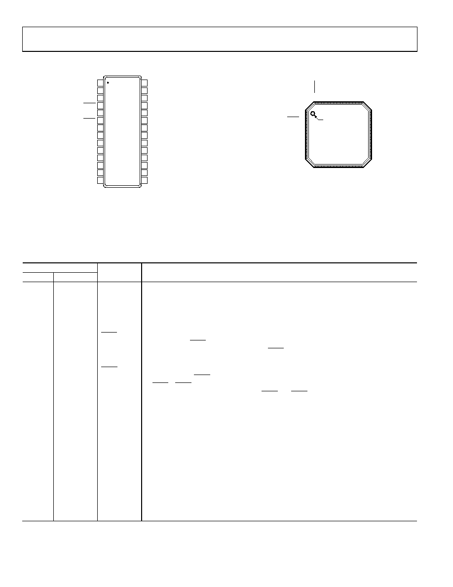
PIN CONFIGURATION AND FUNCTION DESCRIPTIONS
1
2
3
4
5
6
7
8
9
10
11
12
13
14
28
27
26
25
24
23
22
21
20
19
18
17
16
15
SDO
SCLK
SYNC
FAULT
LDAC
SDIN
IODVDD
REGIN
DRIVE
VLOOP
REXT1
REXT2
LOOP–
DVDD
ALARM_CURRENT_DIRECTION
RINT/REXT
COM
RANGE1
RANGE0
CIN
REFOUT1
REFOUT2
REG_SEL1
REG_SEL2
REG_SEL0
REFIN
REGOUT
TOP VIEW
(Not to Scale)
AD5421
NOTES
1. THE EXPOSED PADDLE SHOULD BE CONNECTED TO THE SAME
POTENTIAL AS THE COM PIN AND TO A COPPER PLANE FOR
OPTIMUM THERMAL PERFORMANCE.
09128-
004
Figure 5. TSSOP Pin Configuration
09128-
100
PIN 1
INDICATOR
1
SDIN
2
LDAC
3
FAULT
4
COM
5
DVDD
6
ALARM CURRENT DIRECTION
7
RINT/REXT
8
RANGE 0
24 VLOOP
23 LOOP–
22 REXT2
21 REXT1
20 CIN
19 REFOUT1
18 REFOUT2
17 REFIN
9
RANG
E
1
10
CO
M
11
CO
M
12
NC
13
R
EG
_
SEL
2
14
R
EG
_
SEL
1
15
R
EG
_
SEL
0
16
NC
32
SYN
C
31
S
CL
K
30
S
DO
29
IOD
V
DD
28
RE
G
O
UT
27
RE
G
IN
26
DRI
V
E
25
NC
AD5421
TOP VIEW
(Not to Scale)
NOTES
1. NO CONNECT. DO NOT CONNECT TO THIS PIN.
2. THE EXPOSED PADDLE SHOULD BE CONNECTED TO THE
SAME POTENTIAL AS THE COM PIN AND TO A COPPER
PLANE FOR OPTIMUM THERMAL PERFORMANCE.
Figure 6. LFCSP Pin Configuration
Table 8. Pin Function Descriptions
Pin No.
Mnemonic
Description
TSSOP
LFCSP
1
29
IODVDD
Digital Interface Supply Pin. Digital thresholds are referenced to the voltage applied to this pin. A
voltage from 1.71 V to 5.5 V can be applied to this pin.
2
30
SDO
Serial Data Output. Used to clock data from the input shift register. Data is clocked out on the
rising edge of SCLK and is valid on the falling edge of SCLK.
3
31
SCLK
Serial Clock Input. Data is clocked into the input shift register on the falling edge of SCLK. This
input operates at clock speeds up to 30 MHz.
4
32
SYNC
Frame Synchronization Input, Active Low. This is the frame synchronization signal for the serial
interface. When SYNC is low, data is transferred on the falling edge of SCLK. The input shift
register data is latched on the rising edge of SYNC.
5
1
SDIN
Serial Data Input. Data must be valid on the falling edge of SCLK.
6
2
LDAC
Load DAC Input, Active Low. This pin is used to update the DAC register and, consequently, the
output current. If LDAC is tied permanently low, the DAC register is updated on the rising edge
of SYNC. If LDAC is held high during the write cycle, the input register is updated, but the output
update is delayed until the falling edge of LDAC. The LDAC pin should not be left unconnected.
7
3
FAULT
Fault Alert Output Pin, Active High. This pin is asserted high when a fault is detected. Detectable
faults are loss of SPI interface control, communication error (PEC), loop current out of range,
insufficient loop voltage, and overtemperature. For more information, see the Fault Alerts
section.
8
5
DVDD
3.3 V Digital Power Supply Output. This pin should be decoupled to COM with 100 nF and 4.7 F
capacitors.
9
6
ALARM_
CURRENT_
DIRECTION
Alarm Current Direction Select. This pin is used to select whether the alarm current is upscale
(22.8 mA/24 mA) or downscale (3.2 mA). Connecting this pin to DVDD selects an upscale alarm
current (22.8 mA/24 mA); connecting this pin to COM selects a downscale alarm current (3.2 mA).
For more information, see the Power-On Default section.
10
7
RINT/REXT
Current Setting Resistor Select. When this pin is connected to DVDD, the internal current setting
resistor is selected. When this pin is connected to COM, the external current setting resistor is
selected. An external resistor can be connected between the REXT1 and REXT2 pins.
11, 12
8, 10
RANGE0,
RANGE1
Digital Input Pins. These two pins select the loop current range (see the Loop Current Range
Selection section).
相关PDF资料 |
PDF描述 |
|---|---|
| NR6028T150M | INDUCTOR 15UH 1.8A 20% SMD |
| SC53LC-6R8 | INDUCTOR SMD 6.8UH 1.51A 100KHZ |
| V48C2E50BL3 | CONVERTER MOD DC/DC 2V 50W |
| 0210490844 | CABLE JUMPER 1.25MM .178M 15POS |
| GBC05DREI-S734 | CONN EDGECARD 10POS .100 EYELET |
相关代理商/技术参数 |
参数描述 |
|---|---|
| EVAL-AD5422EBZ | 功能描述:BOARD EVAL FOR AD5422 RoHS:是 类别:编程器,开发系统 >> 评估板 - 数模转换器 (DAC) 系列:- 产品培训模块:Lead (SnPb) Finish for COTS Obsolescence Mitigation Program 标准包装:1 系列:- DAC 的数量:4 位数:12 采样率(每秒):- 数据接口:串行,SPI? 设置时间:3µs DAC 型:电流/电压 工作温度:-40°C ~ 85°C 已供物品:板 已用 IC / 零件:MAX5581 |
| EVAL-AD5422LFEBZ | 功能描述:BOARD EVAL FOR AD5422LFEBZ RoHS:否 类别:编程器,开发系统 >> 评估板 - 数模转换器 (DAC) 系列:* 产品培训模块:Lead (SnPb) Finish for COTS Obsolescence Mitigation Program 标准包装:1 系列:- DAC 的数量:4 位数:12 采样率(每秒):- 数据接口:串行,SPI? 设置时间:3µs DAC 型:电流/电压 工作温度:-40°C ~ 85°C 已供物品:板 已用 IC / 零件:MAX5581 |
| EVAL-AD5424EB | 制造商:Analog Devices 功能描述:EVALUATION BOARD I.C. - Bulk 制造商:Rochester Electronics LLC 功能描述: |
| EVAL-AD5424EBZ | 功能描述:BOARD EVALUATION FOR AD5424 RoHS:是 类别:编程器,开发系统 >> 评估板 - 数模转换器 (DAC) 系列:- 产品培训模块:Lead (SnPb) Finish for COTS Obsolescence Mitigation Program 标准包装:1 系列:- DAC 的数量:4 位数:12 采样率(每秒):- 数据接口:串行,SPI? 设置时间:3µs DAC 型:电流/电压 工作温度:-40°C ~ 85°C 已供物品:板 已用 IC / 零件:MAX5581 |
| EVAL-AD5425EB | 制造商:Analog Devices 功能描述:EVALUATION BOARD I.C. - Bulk |
发布紧急采购,3分钟左右您将得到回复。