- 您现在的位置:买卖IC网 > PDF目录17065 > EVAL-AD5570EBZ (Analog Devices Inc)BOARD EVALUATION FOR AD5570 PDF资料下载
参数资料
| 型号: | EVAL-AD5570EBZ |
| 厂商: | Analog Devices Inc |
| 文件页数: | 11/24页 |
| 文件大小: | 0K |
| 描述: | BOARD EVALUATION FOR AD5570 |
| 标准包装: | 1 |
| DAC 的数量: | 1 |
| 位数: | 16 |
| 采样率(每秒): | 83k |
| 数据接口: | DSP,MICROWIRE?,QSPI?,串行,SPI? |
| 设置时间: | 12µs |
| DAC 型: | 电压 |
| 工作温度: | -40°C ~ 85°C |
| 已供物品: | 板 |
| 已用 IC / 零件: | AD5570 |
AD5570
Rev. C | Page 19 of 24
APPLICATIONS INFORMATION
TYPICAL OPERATING CIRCUIT
Figure 39 shows the typical operating circuit for the AD5570.
The only external component needed for this precision 16-bit
DAC is a single external positive reference. Because the device
incorporates reference buffers, it eliminates the need for a negative
reference, external inverters, precision amplifiers, and resistors.
This leads to an overall savings of both cost and board space.
to ±15 V, but VDD and VSS can operate supplies from 11.4 V to
16.5 V. AGNDS is connected to AGND, but the option of force/
sense is included on this device if required by the user.
1
2
3
4
5
6
7
8
16
15
14
13
12
11
10
9
AD5570
VSS
VDD
CLR
LDAC
SYNC
SCLK
SDIN
SDO
REFGND
REFIN
REFGND
VOUT
AGNDS
AGND
PD
DGND
+15V
0.1F
10F
0.1F
10F
–15V
VOUT
5V
ADR435
LDAC
SYNC
SCLK
SDIN
SDO
5k
0
3760-
044
Figure 39. Typical Operating Circuit
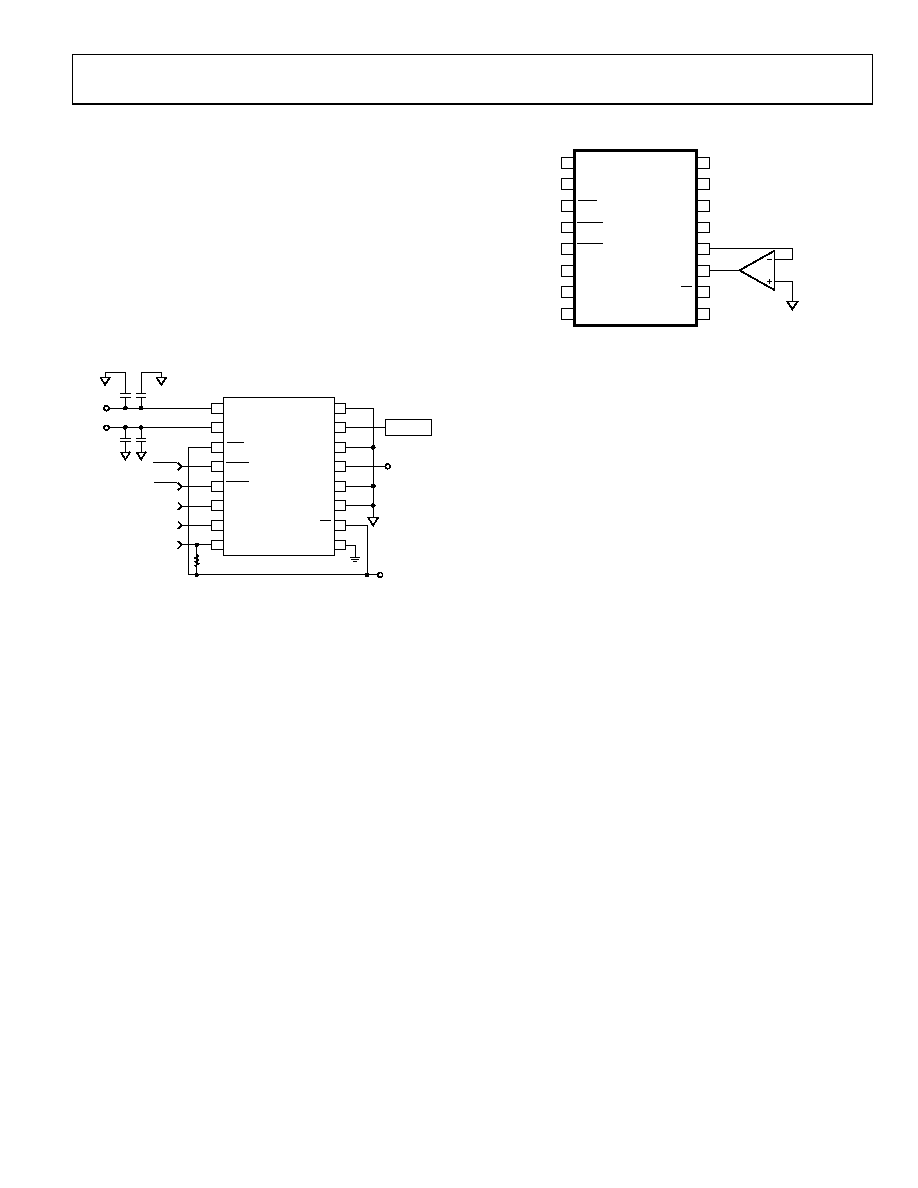
Force/Sense of AGND
Because of the extremely high accuracy of this device, system
design issues (such as grounding and contact resistance) are
very important. The AD5570, with ±10 V output, has an LSB
size of 305 μV. Therefore, series wiring and connector resistances
of very small values can cause voltage drops of an LSB. For this
reason, the AD5570 offers a force/sense output configuration.
Figure 40 shows how to connect the AD5570 to the force/sense
amplifier. Where accuracy of the output is important, an ampli-
fier such as the OP177 is ideal. The OP177 is ultraprecise with
offset voltages of 10 μV maximum at room temperature, and off-
set drift of 0.1 μV/°C maximum. Alternative recommended
amplifiers are the OP1177 and the OP77. For applications where
optimization of the circuit for settling time is needed, the AD845
is recommended.
Precision Voltage Reference Selection
To achieve the optimum performance from the AD5570, give
special attention to the selection of a precision voltage reference.
The AD5570 has just one reference input, REFIN. This voltage
on REFIN is used to provide a buffered positive and negative
reference for the DAC core. Therefore, any error in the voltage
reference is reflected in the output of the device.
6
2
3
(OTHER CONNECTIONS OMITTED
FOR CLARITY)
OP177*
*FOR OPTIMUM SETTLING TIME PERFORMANCE,
THE AD845 IS RECOMMENDED.
03760-045
1
2
3
4
5
6
7
8
16
15
14
13
12
11
10
9
AD5570
VSS
VDD
CLR
LDAC
SYNC
SCLK
SDIN
SDO
REFGND
REFIN
REFGND
VOUT
AGNDS
AGND
PD
DGND
Figure 40. Driving AGND and AGNDS Using a Force/Sense Amplifier
The four possible sources of error to consider when choosing
a voltage reference for high accuracy applications are initial
accuracy, long-term drift, temperature coefficient of the out-
put voltage, and output voltage noise.
Initial accuracy on the output voltage of an external reference can
lead to a full-scale error in the DAC. Therefore, to minimize
these errors, a reference with low initial accuracy specification
is preferred. Also, choosing a reference with an output trim adjust-
ment, such as the ADR425, allows a system designer to trim out
system errors by setting the reference voltage to a voltage other
than the nominal. The trim adjustment can also be used at tem-
perature to trim out any error.
Long-term drift (LTD) is a measure of how much the reference
drifts over time. A reference with a tight long-term drift specifica-
tion ensures that the overall solution remains relatively stable
over its entire lifetime.
The temperature coefficient of a references output voltage
affects INL, DNL, and TUE. Choose a reference with a tight
temperature coefficient specification to reduce the depend
ence of the DAC output voltage on ambient conditions.
In high accuracy applications that have a relatively low noise
budget, reference output voltage noise needs to be considered.
It is important to choose a reference with as low an output noise
voltage as practical for the system resolution required. Precision
voltage references, such as the ADR435 (XFET design), produce
low output noise in the 0.1 Hz to 10 Hz region. However, as the
circuit bandwidth increases, filtering the output of the reference
can be required to minimize the output noise.
相关PDF资料 |
PDF描述 |
|---|---|
| EVAL-AD5379EBZ | BOARD EVALUATION FOR AD5379 |
| EVAL-AD5452EBZ | BOARD EVAL FOR AD5452 |
| EBA22DRMH | CONN EDGECARD 44POS .125 SQ WW |
| ACM03DRXN | CONN EDGECARD 6POS DIP .156 SLD |
| ESA06DTKT-S288 | CONN EDGECARD 12POS .125 EXTEND |
相关代理商/技术参数 |
参数描述 |
|---|---|
| EVAL-AD5570SDZ | 功能描述:BOARD EVAL FOR AD5570 RoHS:是 类别:编程器,开发系统 >> 评估板 - 数模转换器 (DAC) 系列:- 产品培训模块:Lead (SnPb) Finish for COTS Obsolescence Mitigation Program 标准包装:1 系列:- DAC 的数量:4 位数:12 采样率(每秒):- 数据接口:串行,SPI? 设置时间:3µs DAC 型:电流/电压 工作温度:-40°C ~ 85°C 已供物品:板 已用 IC / 零件:MAX5581 |
| EVAL-AD5590EBZ | 功能描述:BOARD EVAL FOR AD5590 RoHS:是 类别:编程器,开发系统 >> 评估板 - 模数转换器 (ADC) 系列:- 产品培训模块:Obsolescence Mitigation Program 标准包装:1 系列:- ADC 的数量:1 位数:12 采样率(每秒):94.4k 数据接口:USB 输入范围:±VREF/2 在以下条件下的电源(标准):- 工作温度:-40°C ~ 85°C 已用 IC / 零件:MAX11645 已供物品:板,软件 |
| EVAL-AD5620EB | 制造商:AD 制造商全称:Analog Devices 功能描述:Single, 12-/14-/16-Bit nanoDAC with 5 ppm/C On-Chip Reference in SOT-23 |
| EVAL-AD5620EBZ | 功能描述:EVAL BOARD FOR AD5620 RoHS:是 类别:编程器,开发系统 >> 评估板 - 数模转换器 (DAC) 系列:nanoDAC™ 产品培训模块:Lead (SnPb) Finish for COTS Obsolescence Mitigation Program 标准包装:1 系列:- DAC 的数量:4 位数:12 采样率(每秒):- 数据接口:串行,SPI? 设置时间:3µs DAC 型:电流/电压 工作温度:-40°C ~ 85°C 已供物品:板 已用 IC / 零件:MAX5581 |
| EVAL-AD5621EBZ | 功能描述:BOARD EVALUATION FOR AD5621 RoHS:是 类别:编程器,开发系统 >> 评估板 - 数模转换器 (DAC) 系列:nanoDAC™ 产品培训模块:Lead (SnPb) Finish for COTS Obsolescence Mitigation Program 标准包装:1 系列:- DAC 的数量:4 位数:12 采样率(每秒):- 数据接口:串行,SPI? 设置时间:3µs DAC 型:电流/电压 工作温度:-40°C ~ 85°C 已供物品:板 已用 IC / 零件:MAX5581 |
发布紧急采购,3分钟左右您将得到回复。