- 您现在的位置:买卖IC网 > PDF目录17065 > EVAL-AD5570EBZ (Analog Devices Inc)BOARD EVALUATION FOR AD5570 PDF资料下载
参数资料
| 型号: | EVAL-AD5570EBZ |
| 厂商: | Analog Devices Inc |
| 文件页数: | 8/24页 |
| 文件大小: | 0K |
| 描述: | BOARD EVALUATION FOR AD5570 |
| 标准包装: | 1 |
| DAC 的数量: | 1 |
| 位数: | 16 |
| 采样率(每秒): | 83k |
| 数据接口: | DSP,MICROWIRE?,QSPI?,串行,SPI? |
| 设置时间: | 12µs |
| DAC 型: | 电压 |
| 工作温度: | -40°C ~ 85°C |
| 已供物品: | 板 |
| 已用 IC / 零件: | AD5570 |
AD5570
Rev. C | Page 16 of 24
GENERAL DESCRIPTION
The AD5570 is a single 16-bit serial input, voltage output DAC. It
operates from supply voltages of ±11.4 V to ±16.5 V, and has a
buffered voltage output of up to ±13.6 V. Data is written to the
AD5570 in a 16-bit word format, via a 3-wire serial interface. The
device also offers an SDO pin, available for daisy-chaining or
readback.
The AD5570 incorporates a power-on reset circuit to ensure the
DAC output powers up to 0 V. The device also has a power-down
pin to reduce the typical current consumption to 16 μA.
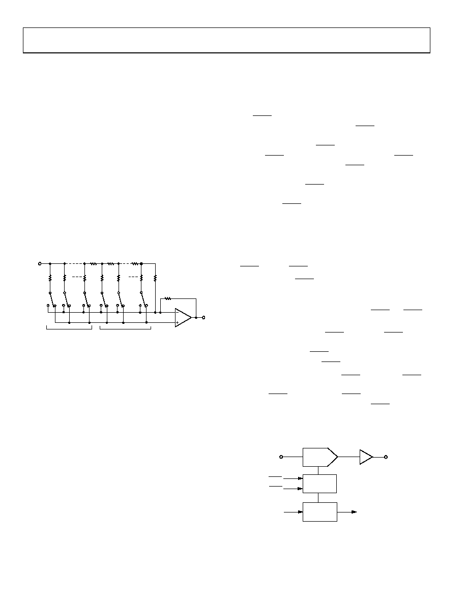
DAC ARCHITECTURE
The DAC architecture of the AD5570 consists of a 16-bit, current-
mode, segmented R-2R DAC. The simplified circuit diagram for
the DAC section is shown in Figure 36.
The four MSBs of the 16-bit data word are decoded to drive
15 switches, E1 to E15. Each of these switches connects one
of the 15 matched resistors to either AGND or IOUT. The
remaining 12 bits of the data word drive switches S0 to S11
of the 12-bit R-2R ladder network.
2R
E15
VREF
2R
E14
E1
2R
S11
RR
R
2R
S10
2R
12-BIT R-2R LADDER
VOUT
2R
S0
2R
AGND
IOUT
R/8
4 MSBs DECODED INTO
15 EQUAL SEGMENTS
03
760
-0
10
Figure 36. DAC Ladder Structure
REFERENCE BUFFERS
The AD5570 operates with an external reference. The reference
input (REFIN) has an input range of up to 7 V. This input voltage is
then used to provide a buffered positive and negative reference
for the DAC core. The positive reference is given by
REFIN
REF
V
×
=
+
2
and the negative reference to the DAC core is given by
REFIN
REF
V
×
=
2
These positive and negative reference voltages define the DAC
output range.
SERIAL INTERFACE
The AD5570 is controlled over a versatile 3-wire serial interface
that operates at clock rates up to 10 MHz and is compatible with
SPI, QSPI, MICROWIRE, and DSP interface standards.
Input Shift Register
The input shift register is 16 bits wide. Data is loaded into the
device as a 16-bit word under the control of a serial clock input,
SCLK. The timing diagram for this operation is shown in Figure 2.
On power-up, the input shift register and DAC register are
loaded with midscale (0x8000). The DAC coding is straight
binary; all 0s produce an output of 2 VREF; all 1s produce an
output of +2 VREF 1 LSB.
The SYNC input is a level-triggered input that acts as a frame
synchronization signal and chip enable. SYNC must frame the
serial word being loaded into the device. Data can be transferred
into the device only while SYNCis low. To start the serial data
transfer, SYNC is taken low, observing the minimum SYNC to
SCLK falling edge setup time, t4. After SYNC goes low, serial data
on SDIN is shifted into the device’s input shift register on the
falling edges of SCLK. SYNC can be taken high after the falling
edge of the 16th SCLK pulse, observing the minimum SCLK
falling edge to SYNC rising edge time, t7.
After the end of the serial data transfer, data is automatically
transferred from the input shift register to the input register
of the DAC.
When data has been transferred into the input register of the DAC,
the DAC register and DAC output can be updated by taking
LDAC low while SYNC is high.
Load DAC Input (LDAC)
There are two ways that the DAC register and DAC output can
be updated when data has been transferred into the input register
of the DAC. Depending on the status of both SYNC and LDAC,
one of two update modes is selected.
The first mode is synchronous LDAC. In this mode, LDAC is low
while data is being clocked into the input shift register. The DAC
output is updated when SYNC is taken high. The update here
occurs on the rising edge of SYNC.
The second mode is asynchronous LDAC. In this mode, LDAC
is high while data is being clocked in. The DAC output is updated
by taking LDAC low any time after SYNC has been taken high.
The update now occurs on the falling edge of LDAC.
Figure 37 shows a simplified block diagram of the input loading
circuitry.
VOUT
DAC
REGISTER
INPUT SHIFT
REGISTER
OUTPUT
I/V AMPLIFIER
LDAC
SDO
SDIN
16-BIT
DAC
VREFIN
SYNC
03760-012
Figure 37. Simplified Serial Interface Showing Input Loading Circuitry
相关PDF资料 |
PDF描述 |
|---|---|
| EVAL-AD5379EBZ | BOARD EVALUATION FOR AD5379 |
| EVAL-AD5452EBZ | BOARD EVAL FOR AD5452 |
| EBA22DRMH | CONN EDGECARD 44POS .125 SQ WW |
| ACM03DRXN | CONN EDGECARD 6POS DIP .156 SLD |
| ESA06DTKT-S288 | CONN EDGECARD 12POS .125 EXTEND |
相关代理商/技术参数 |
参数描述 |
|---|---|
| EVAL-AD5570SDZ | 功能描述:BOARD EVAL FOR AD5570 RoHS:是 类别:编程器,开发系统 >> 评估板 - 数模转换器 (DAC) 系列:- 产品培训模块:Lead (SnPb) Finish for COTS Obsolescence Mitigation Program 标准包装:1 系列:- DAC 的数量:4 位数:12 采样率(每秒):- 数据接口:串行,SPI? 设置时间:3µs DAC 型:电流/电压 工作温度:-40°C ~ 85°C 已供物品:板 已用 IC / 零件:MAX5581 |
| EVAL-AD5590EBZ | 功能描述:BOARD EVAL FOR AD5590 RoHS:是 类别:编程器,开发系统 >> 评估板 - 模数转换器 (ADC) 系列:- 产品培训模块:Obsolescence Mitigation Program 标准包装:1 系列:- ADC 的数量:1 位数:12 采样率(每秒):94.4k 数据接口:USB 输入范围:±VREF/2 在以下条件下的电源(标准):- 工作温度:-40°C ~ 85°C 已用 IC / 零件:MAX11645 已供物品:板,软件 |
| EVAL-AD5620EB | 制造商:AD 制造商全称:Analog Devices 功能描述:Single, 12-/14-/16-Bit nanoDAC with 5 ppm/C On-Chip Reference in SOT-23 |
| EVAL-AD5620EBZ | 功能描述:EVAL BOARD FOR AD5620 RoHS:是 类别:编程器,开发系统 >> 评估板 - 数模转换器 (DAC) 系列:nanoDAC™ 产品培训模块:Lead (SnPb) Finish for COTS Obsolescence Mitigation Program 标准包装:1 系列:- DAC 的数量:4 位数:12 采样率(每秒):- 数据接口:串行,SPI? 设置时间:3µs DAC 型:电流/电压 工作温度:-40°C ~ 85°C 已供物品:板 已用 IC / 零件:MAX5581 |
| EVAL-AD5621EBZ | 功能描述:BOARD EVALUATION FOR AD5621 RoHS:是 类别:编程器,开发系统 >> 评估板 - 数模转换器 (DAC) 系列:nanoDAC™ 产品培训模块:Lead (SnPb) Finish for COTS Obsolescence Mitigation Program 标准包装:1 系列:- DAC 的数量:4 位数:12 采样率(每秒):- 数据接口:串行,SPI? 设置时间:3µs DAC 型:电流/电压 工作温度:-40°C ~ 85°C 已供物品:板 已用 IC / 零件:MAX5581 |
发布紧急采购,3分钟左右您将得到回复。