- 您现在的位置:买卖IC网 > PDF目录17076 > EVAL-AD5570SDZ (Analog Devices Inc)BOARD EVAL FOR AD5570 PDF资料下载
参数资料
| 型号: | EVAL-AD5570SDZ |
| 厂商: | Analog Devices Inc |
| 文件页数: | 14/24页 |
| 文件大小: | 0K |
| 描述: | BOARD EVAL FOR AD5570 |
| 标准包装: | 1 |
| DAC 的数量: | 1 |
| 位数: | 16 |
| 采样率(每秒): | 83k |
| 数据接口: | DSP,MICROWIRE?,QSPI?,串行,SPI? |
| 设置时间: | 12µs |
| DAC 型: | 电压 |
| 工作温度: | -40°C ~ 85°C |
| 已供物品: | 板 |
| 已用 IC / 零件: | AD5570 |
AD5570
Rev. C | Page 21 of 24
MICROPROCESSOR INTERFACING
Microprocessor interfacing to the AD5570 is via a serial bus
that uses standard protocol compatible with microcontrollers
and DSP processors. The communications channel is a 3-wire
(minimum) interface consisting of a clock signal, a data signal,
and a synchronization signal. The AD5570 requires a 16-bit
data word with data valid on the falling edge of SCLK.
For all the interfaces, the DAC output update can be done auto-
matically when all the data is clocked in, or it can be done under
the control of LDAC. The contents of the DAC register can be
read using the readback function.
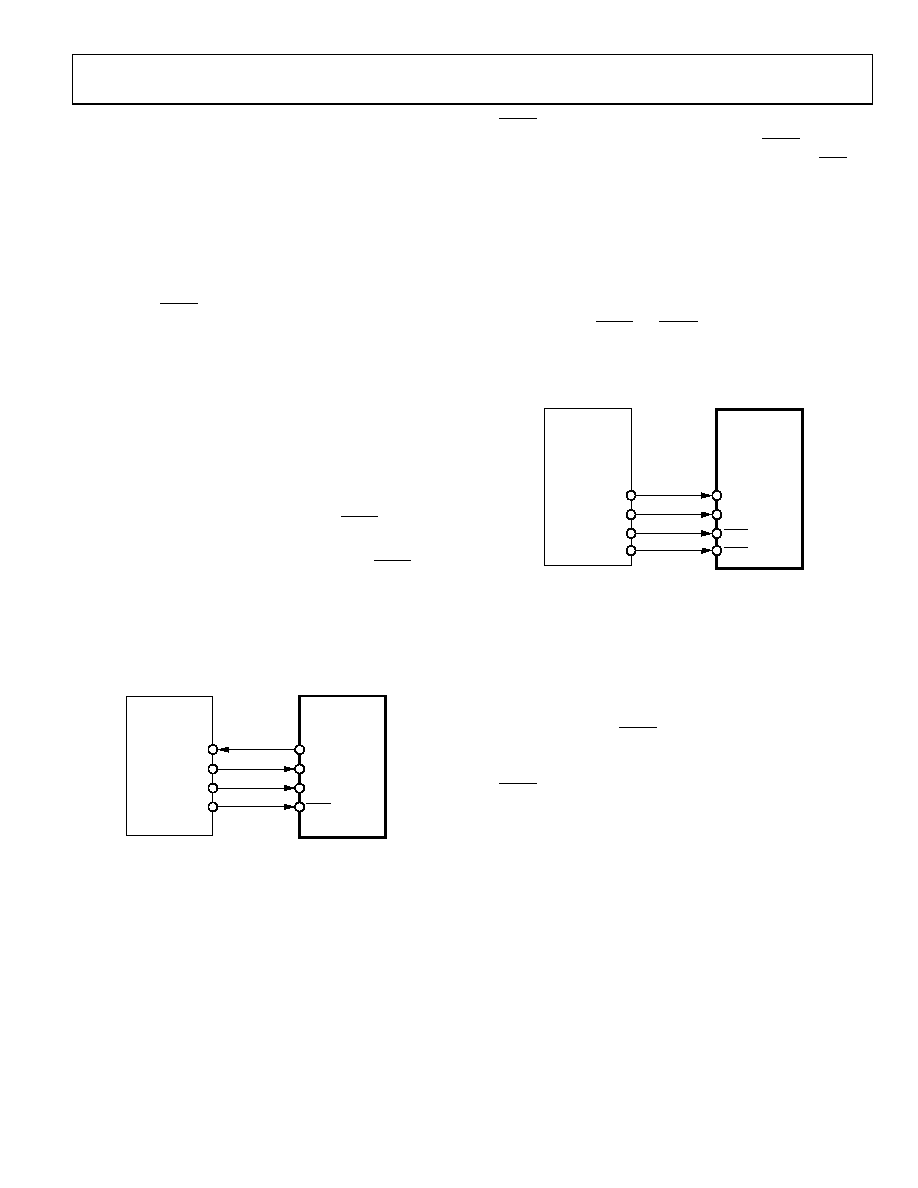
AD5570 to MC68HC11 Interface
Figure 42 shows an example of a serial interface between the
AD5570 and the MC68HC11 microcontroller. The serial periph-
eral interface (SPI) on the MC68HC11 is configured for master
mode (MSTR = 1), clock polarity bit (CPOL = 0), and the clock
phase bit (CPHA = 1). The SPI is configured by writing to the SPI
control register (SPCR); see documentation on the MC68HC11.
SCK of the MC68HC11 drives the SCLK of the AD5570, the
MOSI output drives the serial data line (SDIN) of the AD5570,
and the MISO input is driven from SDO. The SYNC is driven
from one of the port lines, in this case, PC7.
When data is being transmitted to the AD5570, the SYNC line
(PC7) is taken low and data is transmitted MSB first. Data appear-
ing on the MOSI output is valid on the falling edge of SCK. Eight
falling clock edges occur in the transmit cycle; therefore, in order
to load the required 16-bit word, PC7 is not brought high until
the second 8-bit word has been transferred to the DACs input
shift register.
AD5570*
SCLK
SDIN
SYNC
MOSI
SCLK
PC7
MC68HC11*
*ADDITIONAL PINS OMITTED FOR CLARITY.
SDO
MISO
03
76
0-
01
4
Figure 42. AD5570 to MC68HC11 Interface
LDAC is controlled by the PC6 port output. The DAC can be
updated after each 2-byte transfer by bringing LDAC low. This
example does not show other serial lines for the DAC. If CLR
were used, control it by the Port Output PC5.
AD5570 to 8xC51 Interface
The AD5570 requires a clock synchronized to the serial data. For
this reason, the 8xC51 must be operated in Mode 0. In this mode,
serial data enters and exits through RxD, and a shift clock is
output on TxD.
P3.3 and P3.4 are bit-programmable pins on the serial port and
are used to drive SYNC and LDAC, respectively.
The 8xC51 provides the LSB of its SBUF register as the first bit
in the data stream. The user must ensure that the data in the SBUF
register is arranged correctly because the DAC expects MSB first.
AD5570*
SCLK
SDIN
SYNC
TxD
P3.3
8xC51*
*ADDITIONAL PINS OMITTED FOR CLARITY.
RxD
LDAC
P3.4
03
76
0-
01
5
Figure 43. AD5570 to 8xC51 Interface
When data is to be transmitted to the DAC, P3.3 is taken low. Data
on RxD is clocked out of the microcontroller on the rising edge
of TxD and is valid on the falling edge. As a result, no glue logic
is required between this DAC and the microcontroller interface.
The 8xC51 transmits data in 8-bit bytes with only eight falling
clock edges occurring in the transmit cycle. Because the DAC
expects a 16-bit word, SYNC (P3.3) must be left low after the first
eight bits are transferred. After the second byte has been trans-
ferred, the P3.3 line is taken high. The DAC can be updated using
LDAC via P3.4 of the 8xC51.
相关PDF资料 |
PDF描述 |
|---|---|
| FPF2006 | IC SWITCH LOAD FULL FUNC SC70-5 |
| UCS2G680MNY9 | CAP ALUM 68UF 400V 20% RADIAL |
| UPB2D391MRD | CAP ALUM 390UF 200V 20% RADIAL |
| MIC94095YMT TR | IC LOAD SW HGH SIDE 1.2A 4-TMLF |
| LGU2G121MELZ | CAP ALUM 120UF 400V 20% SNAP |
相关代理商/技术参数 |
参数描述 |
|---|---|
| EVAL-AD5590EBZ | 功能描述:BOARD EVAL FOR AD5590 RoHS:是 类别:编程器,开发系统 >> 评估板 - 模数转换器 (ADC) 系列:- 产品培训模块:Obsolescence Mitigation Program 标准包装:1 系列:- ADC 的数量:1 位数:12 采样率(每秒):94.4k 数据接口:USB 输入范围:±VREF/2 在以下条件下的电源(标准):- 工作温度:-40°C ~ 85°C 已用 IC / 零件:MAX11645 已供物品:板,软件 |
| EVAL-AD5620EB | 制造商:AD 制造商全称:Analog Devices 功能描述:Single, 12-/14-/16-Bit nanoDAC with 5 ppm/C On-Chip Reference in SOT-23 |
| EVAL-AD5620EBZ | 功能描述:EVAL BOARD FOR AD5620 RoHS:是 类别:编程器,开发系统 >> 评估板 - 数模转换器 (DAC) 系列:nanoDAC™ 产品培训模块:Lead (SnPb) Finish for COTS Obsolescence Mitigation Program 标准包装:1 系列:- DAC 的数量:4 位数:12 采样率(每秒):- 数据接口:串行,SPI? 设置时间:3µs DAC 型:电流/电压 工作温度:-40°C ~ 85°C 已供物品:板 已用 IC / 零件:MAX5581 |
| EVAL-AD5621EBZ | 功能描述:BOARD EVALUATION FOR AD5621 RoHS:是 类别:编程器,开发系统 >> 评估板 - 数模转换器 (DAC) 系列:nanoDAC™ 产品培训模块:Lead (SnPb) Finish for COTS Obsolescence Mitigation Program 标准包装:1 系列:- DAC 的数量:4 位数:12 采样率(每秒):- 数据接口:串行,SPI? 设置时间:3µs DAC 型:电流/电压 工作温度:-40°C ~ 85°C 已供物品:板 已用 IC / 零件:MAX5581 |
| EVAL-AD5629REBRZ | 功能描述:BOARD EVAL FOR AD5629 TSSOP RoHS:是 类别:编程器,开发系统 >> 评估板 - 数模转换器 (DAC) 系列:denseDAC 产品培训模块:Lead (SnPb) Finish for COTS Obsolescence Mitigation Program 标准包装:1 系列:- DAC 的数量:4 位数:12 采样率(每秒):- 数据接口:串行,SPI? 设置时间:3µs DAC 型:电流/电压 工作温度:-40°C ~ 85°C 已供物品:板 已用 IC / 零件:MAX5581 |
发布紧急采购,3分钟左右您将得到回复。