- 您现在的位置:买卖IC网 > PDF目录17030 > EVAL-AD5590EBZ (Analog Devices Inc)BOARD EVAL FOR AD5590 PDF资料下载
参数资料
| 型号: | EVAL-AD5590EBZ |
| 厂商: | Analog Devices Inc |
| 文件页数: | 29/44页 |
| 文件大小: | 0K |
| 描述: | BOARD EVAL FOR AD5590 |
| 标准包装: | 1 |
| ADC 的数量: | 1 |
| 位数: | 12 |
| 采样率(每秒): | 1M |
| 数据接口: | 串行 |
| 输入范围: | 2 Vpp |
| 在以下条件下的电源(标准): | 12.5mW @ 1MSPS,5V |
| 工作温度: | -40°C ~ 85°C |
| 已用 IC / 零件: | AD5590 |
| 已供物品: | 板 |
第1页第2页第3页第4页第5页第6页第7页第8页第9页第10页第11页第12页第13页第14页第15页第16页第17页第18页第19页第20页第21页第22页第23页第24页第25页第26页第27页第28页当前第29页第30页第31页第32页第33页第34页第35页第36页第37页第38页第39页第40页第41页第42页第43页第44页
AD5590
Rev. A | Page 35 of 44
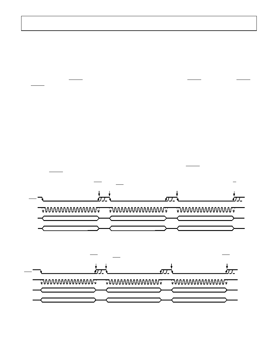
AutoShutdown (PM1 = 0, PM0 = 1)
In this mode, the ADC automatically enters shutdown at the
end of each conversion when the ADC control register is updated.
When the ADC is in shutdown, the track-and-hold is in hold
mode. Figure 66 shows the general diagram of the operation of
the ADC in this mode. In shutdown mode, all internal circuitry
on the ADC is powered down. The ADC retains information in
the ADC control register during shutdown. The ADC remains
in shutdown until the next ASYNC falling edge it receives. On
this ASYNC falling edge, the track-and-hold that was in hold
while the ADC was in shutdown returns to track. Wake-up time
from autoshutdown is 1 s, and the user should ensure that 1 s
has elapsed before attempting a valid conversion. When running
the ADC with a 20 MHz clock, one dummy cycle of 16 × ASCLKs
should be sufficient to ensure that the ADC is fully powered up.
During this dummy cycle, the contents of the ADC control
register should remain unchanged; therefore, the write bit
should be 0 on the ADIN line. This dummy cycle effectively
halves the throughput rate of the ADC, with every other
conversion result being valid. In this mode, the power
consumption of the ADC is greatly reduced with the ADC
entering shutdown at the end of each conversion. When the
ADC control register is programmed to move into
autoshutdown, it does so at the end of the conversion. The user
can move the ADC in and out of the low power state by
controlling the ASYNC signal.
Autostandby (PM1 = PM0 = 0)
In this mode, the ADC automatically enters standby mode at
the end of each conversion when the ADC control register is
updated. Figure 67 shows the general diagram of the operation
of the ADC in this mode. When the ADC is in standby, portions
of the ADC are powered down, but the on-chip bias generator
remains powered up. The ADC retains information in the ADC
control register during standby. The ADC remains in standby
until it receives the next ASYNC falling edge. On this ASYNC
falling edge, the track and hold that was in hold while the ADC
was in standby returns to track. Wake-up time from standby is 1
s; the user should ensure that 1 s has elapsed before attempting a
valid conversion on the ADC in this mode. When running the
ADC with a 20 MHz clock, one dummy cycle of 16 × ASCLKs
should be sufficient to ensure the ADC is fully powered up.
During this dummy cycle, the contents of the ADC control register
should remain unchanged; therefore, the write bit should be set
to 0 on the ADIN line. This dummy cycle effectively halves the
throughput rate of the ADC with every other conversion result
being valid. In this mode, the power consumption of the ADC
is greatly reduced with the ADC entering standby at the end of
each conversion. When the ADC control register is programmed
to move into autostandby, it does so at the end of the conver-
sion. The user can move the ADC in and out of the low power
state by controlling the ASYNC signal.
ASCLK
1
16
1
16
1
16
ADOUT
ADIN
ASYNC
DUMMY CONVERSION
CONTROL REGISTER IS LOADED ON THE
FIRST 12 CLOCKS, PM1 = 0, PM0 = 1
CONTROL REGISTER CONTENTS SHOULD
NOT CHANGE, WRITE BIT = 0
PART ENTERS
SHUTDOWN ON CS
RISING EDGE AS
PM1 = 0, PM0 = 1
PART IS FULLY
POWERED UP
TO KEEP PART IN THIS MODE, LOAD PM1 = 0, PM0 = 1
IN CONTROL REGISTER OR SET WRITE BIT = 0
CHANNEL IDENTIFIER BITS + CONVERSION RESU
LT
DATA IN TO CONTROL/SHADOW REGISTER
CHANNEL IDENTIFIER BITS + CONVERSION RESU
LT
DATA IN TO CONTROL/SHADOW REGISTER
INVALID DATA
PART ENTERS
SHUTDOWN ON ASYNC
RISING EDGE AS
PM1 = 0, PM0 = 1
PART BEGINS
TO POWER
UP ON ASYNC
FALLING EDGE
07691-
066
Figure 66. Autoshutdown Mode Operation
ASCLK
1
12
16
1
12
16
1
12
16
ADOUT
ADIN
ASYNC
DUMMY CONVERSION
CONTROL REGISTER IS LOADED ON THE
FIRST 12 CLOCKS, PM1 = 0, PM0 = 0
CONTROL REGISTER CONTENTS SHOULD
REMAIN UNCHANGED, WRITE BIT = 0
PART IS FULLY
POWERED UP
TO KEEP PART IN THIS MODE, LOAD PM1 = 0,
PM0 = 0 IN CONTROL REGISTER
PART ENTERS
STANDBY ON ASYNC
RISING EDGE AS
PM1 = 0, PM0 = 0
PART ENTERS
STANDBY ON ASYNC
RISING EDGE AS
PM1 = 0, PM0 = 0
PART BEGINS
TO POWER
UP ON ASYNC
FALLING EDGE
CHANNEL IDENTIFIER BITS + CONVERSION RESULT
INVALID DATA
DATA IN TO CONTROL/SHADOW REGISTER
07691-
067
Figure 67. Autostandby Mode Operation
相关PDF资料 |
PDF描述 |
|---|---|
| EVAL-AD7657-1EDZ | BOARD EVAL CONTROL AD7657-1 |
| VI-B71-EY | CONVERTER MOD DC/DC 12V 50W |
| PCMC135T-1R0MF | COIL 1.0 UH POWER CHOKE 20% SMD |
| SDR0703-680KL | INDUCTOR POWER 68UH SMD |
| EVAL-AD7656-1EDZ | BOARD EVAL CONTROL AD7656-1 |
相关代理商/技术参数 |
参数描述 |
|---|---|
| EVAL-AD5620EB | 制造商:AD 制造商全称:Analog Devices 功能描述:Single, 12-/14-/16-Bit nanoDAC with 5 ppm/C On-Chip Reference in SOT-23 |
| EVAL-AD5620EBZ | 功能描述:EVAL BOARD FOR AD5620 RoHS:是 类别:编程器,开发系统 >> 评估板 - 数模转换器 (DAC) 系列:nanoDAC™ 产品培训模块:Lead (SnPb) Finish for COTS Obsolescence Mitigation Program 标准包装:1 系列:- DAC 的数量:4 位数:12 采样率(每秒):- 数据接口:串行,SPI? 设置时间:3µs DAC 型:电流/电压 工作温度:-40°C ~ 85°C 已供物品:板 已用 IC / 零件:MAX5581 |
| EVAL-AD5621EBZ | 功能描述:BOARD EVALUATION FOR AD5621 RoHS:是 类别:编程器,开发系统 >> 评估板 - 数模转换器 (DAC) 系列:nanoDAC™ 产品培训模块:Lead (SnPb) Finish for COTS Obsolescence Mitigation Program 标准包装:1 系列:- DAC 的数量:4 位数:12 采样率(每秒):- 数据接口:串行,SPI? 设置时间:3µs DAC 型:电流/电压 工作温度:-40°C ~ 85°C 已供物品:板 已用 IC / 零件:MAX5581 |
| EVAL-AD5629REBRZ | 功能描述:BOARD EVAL FOR AD5629 TSSOP RoHS:是 类别:编程器,开发系统 >> 评估板 - 数模转换器 (DAC) 系列:denseDAC 产品培训模块:Lead (SnPb) Finish for COTS Obsolescence Mitigation Program 标准包装:1 系列:- DAC 的数量:4 位数:12 采样率(每秒):- 数据接口:串行,SPI? 设置时间:3µs DAC 型:电流/电压 工作温度:-40°C ~ 85°C 已供物品:板 已用 IC / 零件:MAX5581 |
| EVAL-AD5629RSDZ | 功能描述:BOARD EVAL FOR AD5629 RoHS:是 类别:编程器,开发系统 >> 评估板 - 数模转换器 (DAC) 系列:denseDAC 产品培训模块:Lead (SnPb) Finish for COTS Obsolescence Mitigation Program 标准包装:1 系列:- DAC 的数量:4 位数:12 采样率(每秒):- 数据接口:串行,SPI? 设置时间:3µs DAC 型:电流/电压 工作温度:-40°C ~ 85°C 已供物品:板 已用 IC / 零件:MAX5581 |
发布紧急采购,3分钟左右您将得到回复。