- 您现在的位置:买卖IC网 > PDF目录17048 > EVAL-AD7328SDZ (Analog Devices Inc)BOARD EVAL FOR AD7328 PDF资料下载
参数资料
| 型号: | EVAL-AD7328SDZ |
| 厂商: | Analog Devices Inc |
| 文件页数: | 8/37页 |
| 文件大小: | 0K |
| 描述: | BOARD EVAL FOR AD7328 |
| 标准包装: | 1 |
| 系列: | iCMOS® |
| ADC 的数量: | 1 |
| 位数: | 12 |
| 采样率(每秒): | 1M |
| 数据接口: | DSP,MICROWIRE?,QSPI?,串行,SPI? |
| 输入范围: | ±10 V |
| 在以下条件下的电源(标准): | 31mW @ 1MSPS |
| 工作温度: | -40°C ~ 85°C |
| 已用 IC / 零件: | AD7328 |
| 已供物品: | 板 |
第1页第2页第3页第4页第5页第6页第7页当前第8页第9页第10页第11页第12页第13页第14页第15页第16页第17页第18页第19页第20页第21页第22页第23页第24页第25页第26页第27页第28页第29页第30页第31页第32页第33页第34页第35页第36页第37页
Data Sheet
AD7328
Rev. C | Page 15 of 36
THEORY OF OPERATION
CIRCUIT INFORMATION
The AD7328 is a fast, 8-channel, 12-bit plus sign, bipolar input,
serial ADC. The AD7328 can accept bipolar input ranges that
include ±10 V, ±5 V, and ±2.5 V; it can also accept a 0 V to +10 V
unipolar input range. A different analog input range can be
programmed on each analog input channel via the on-chip
registers. The AD7328 has a high speed serial interface that
can operate at throughput rates up to 1 MSPS.
voltage analog input structures. These supplies must be equal
to or greater than the analog input range. See Table 6 for the
requirements of these supplies for each analog input range. The
power the ADC core.
Table 6. Reference and Supply Requirements for Each
Analog Input Range
Selected Analog
Input Range (V)
Reference
Voltage (V)
Full-Scale
Input
Range (V)
VCC (V)
Minimum
VDD/VSS
(V)1
±10
2.5
±10
3/5
±10
3.0
±12
3/5
±12
±5
2.5
±5
3/5
±5
3.0
±6
3/5
±6
±2.5
2.5
±2.5
3/5
±5
3.0
±3
3/5
±5
0 to +10
2.5
0 to +10
3/5
+10/AGND
3.0
0 to +12
3/5
+12/AGND
1
Guaranteed performance for VDD = 12 V to 16.5 V and VSS = 12 V to 16.5 V.
The performance specifications are guaranteed for VDD = 12 V
to 16.5 V and VSS = 12 V to 16.5 V. With VDD and VSS supplies
outside this range, the AD7328 is fully functional but performance
is not guaranteed. When the AD7328 is configured with the
minimum VDD and VSS supplies for a chosen analog input range,
the throughput rate should be decreased from the maximum
throughput range (see the Typical Performance Characteristics
section). Figure 18 and Figure 19 show the change in INL and
DNL as the VDD and VSS voltages are varied. When operating at
the maximum throughput rate, as the VDD and VSS supply voltages
are reduced, the INL and DNL error increases. However, as the
throughput rate is reduced with the minimum VDD and VSS
supplies, the INL and DNL error is reduced.
are reduced. At the maximum throughput rate, the THD degrades
significantly as VDD and VSS are reduced. It is therefore necessary to
reduce the throughput rate when using minimum VDD and VSS
supplies so that there is less degradation of THD and the specified
performance can be maintained. The degradation is due to an
increase in the on resistance of the input multiplexer when the
VDD and VSS supplies are reduced.
The analog inputs can be configured as eight single-ended inputs,
four true differential input pairs, four pseudo differential inputs,
or seven pseudo differential inputs. Selection can be made by
programming the mode bits, Mode 0 and Mode 1, in the control
register.
The serial clock input accesses data from the part and provides the
clock source for the successive approximation ADC. The AD7328
has an on-chip 2.5 V reference. However, the AD7328 can also
work with an external reference. On power-up, the external
reference operation is the default option. If the internal reference
is preferable, the user must write to the reference bit in the
control register to select the internal reference operation.
The AD7328 also features power-down options to allow power
savings between conversions. The power-down modes are selected
by programming the on-chip control register as described in the
Modes of Operation section.
CONVERTER OPERATION
The AD7328 is a successive approximation analog-to-digital
converter built around two capacitive DACs. Figure 23 and
Figure 24 show simplified schematics of the ADC in single-
ended mode during the acquisition and conversion phases,
respectively. Figure 25 and Figure 26 show simplified schematics
of the ADC in differential mode during acquisition and conversion
phases, respectively.
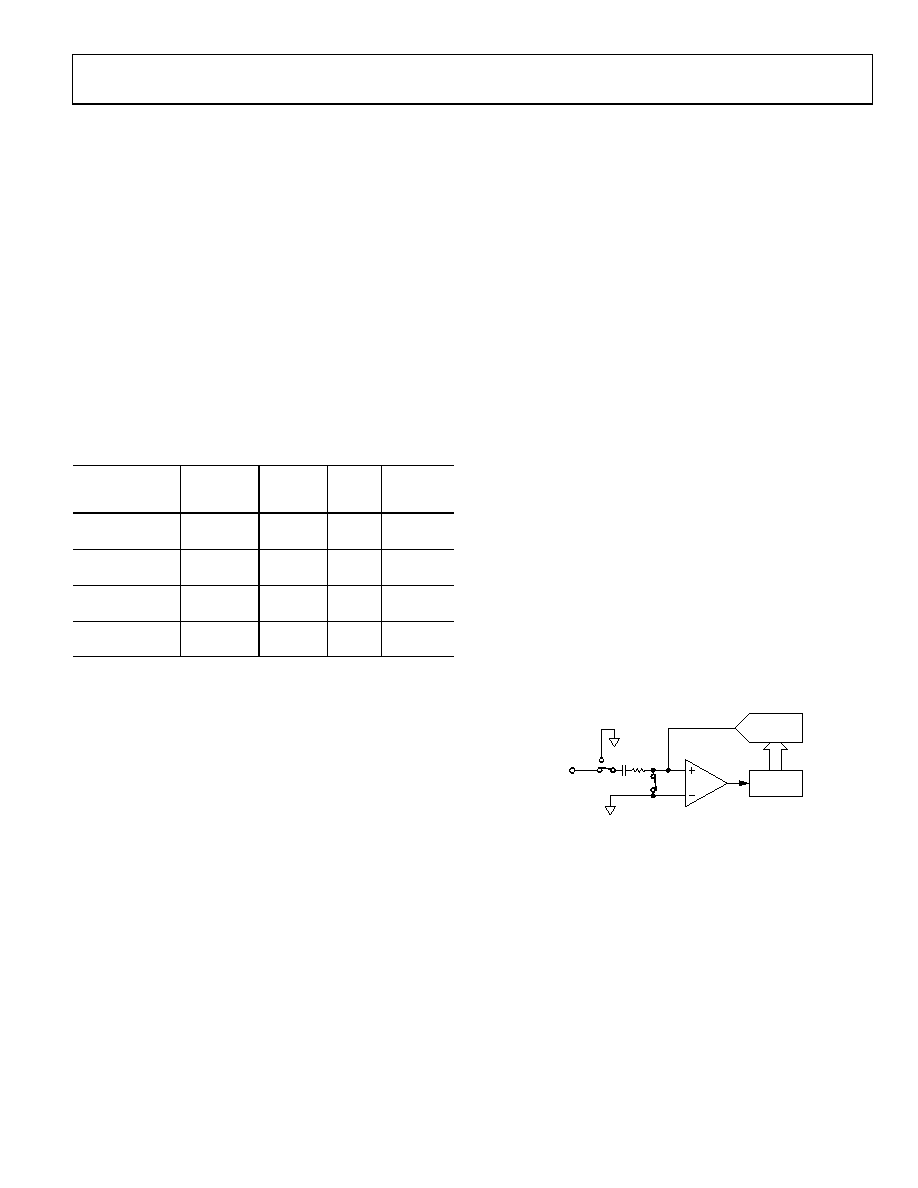
The ADC is composed of control logic, a SAR, and capacitive
DACs. In Figure 23 (the acquisition phase), SW2 is closed and
SW1 is in Position A, the comparator is held in a balanced con-
dition, and the sampling capacitor array acquires the signal on
the input.
CAPACITIVE
DAC
CONTROL
LOGIC
COMPARATOR
AGND
SW2
SW1
A
B
CS
VIN0
04852-
017
Figure 23. ADC Configuration During Acquisition Phase, Single-Ended Mode
When the ADC starts a conversion (see Figure 24), SW2 opens and
SW1 moves to Position B, causing the comparator to become
unbalanced. The control logic and the charge redistribution
DAC are used to add and subtract fixed amounts of charge from
the capacitive DAC to bring the comparator back into a balanced
condition. When the comparator is rebalanced, the conversion
is complete. The control logic generates the ADC output code.
相关PDF资料 |
PDF描述 |
|---|---|
| ESC06DRTH-S734 | CONN EDGECARD 12POS DIP .100 SLD |
| ECC31DCAI | CONN EDGECARD 62POS R/A .100 SLD |
| EVAL-AD7276SDZ | BOARD EVAL FOR AD7276 |
| ABC05DRYS | CONN EDGECARD 10POS .100 DIP SLD |
| ESC06DREI-S734 | CONN EDGECARD 12POS .100 EYELET |
相关代理商/技术参数 |
参数描述 |
|---|---|
| EVAL-AD7329CB | 制造商:Analog Devices 功能描述: |
| EVAL-AD7329CBZ | 功能描述:BOARD EVALUATION FOR AD7329CBZ RoHS:是 类别:编程器,开发系统 >> 评估板 - 模数转换器 (ADC) 系列:iCMOS® 产品培训模块:Obsolescence Mitigation Program 标准包装:1 系列:- ADC 的数量:1 位数:12 采样率(每秒):94.4k 数据接口:USB 输入范围:±VREF/2 在以下条件下的电源(标准):- 工作温度:-40°C ~ 85°C 已用 IC / 零件:MAX11645 已供物品:板,软件 |
| EVAL-AD73311EB | 制造商:AD 制造商全称:Analog Devices 功能描述:Low Cost, Low Power CMOS General Purpose Analog Front End |
| EVAL-AD73311EZ | 制造商:AD 制造商全称:Analog Devices 功能描述:Low Cost, Low Power CMOS General Purpose Analog Front End |
| EVAL-AD73311LEB | 制造商:AD 制造商全称:Analog Devices 功能描述:Low Cost, Low Power CMOS General Purpose Analog Front End |
发布紧急采购,3分钟左右您将得到回复。