- 您现在的位置:买卖IC网 > PDF目录17053 > EVAL-AD7450CBZ (Analog Devices Inc)BOARD EVALUATION FOR AD7450 PDF资料下载
参数资料
| 型号: | EVAL-AD7450CBZ |
| 厂商: | Analog Devices Inc |
| 文件页数: | 17/22页 |
| 文件大小: | 0K |
| 描述: | BOARD EVALUATION FOR AD7450 |
| 标准包装: | 1 |
| ADC 的数量: | 1 |
| 位数: | 12 |
| 采样率(每秒): | 1M |
| 数据接口: | DSP,MICROWIRE?,QSPI?,串行,SPI? |
| 输入范围: | ±VREF/2 |
| 在以下条件下的电源(标准): | 9mW @ 1MSPS |
| 工作温度: | -40°C ~ 85°C |
| 已用 IC / 零件: | AD7450 |
| 已供物品: | 板,CD |
| 相关产品: | AD7450BRZ-ND - IC ADC 12BIT DIFF IN 1MSPS 8SOIC AD7450BRMZ-ND - IC ADC 12BIT DIFF IN 1MSPS 8MSOP AD7450ARMZ-ND - IC ADC 12BIT DIFF IN 1MSPS 8MSOP AD7450ABRMZ-ND - IC ADC 12BIT DIFF IN 1MSPS 8MSOP AD7450ARZ-REEL7-ND - IC ADC 12BIT DIFF IN 1MSPS 8SOIC AD7450ARMZ-REEL7-ND - IC ADC 12BIT DIFF IN 1MSPS 8MSOP AD7450ABRTZ-REEL7TR-ND - IC ADC 12BIT DIFF 1MSPS SOT23-8 AD7450ARZ-REEL-ND - IC ADC 12BIT DIFF IN 1MSPS 8SOIC AD7450ARZ-ND - IC ADC 12BIT DIFF-IN 1MSPS 8SOIC AD7450ABRT-R2CT-ND - IC ADC 12BIT W/DIFF INP SOT-23-8 更多... |
–4–
AD7450
Limit at TMIN, TMAX
Parameter
3 V
5 V
Unit
Description
fSCLK
4
50
kHz min
15
18
MHz max
tCONVERT
16
tSCLK
16
tSCLK
tSCLK = 1/fSCLK
1.07
0.88
s max
SCLK = 15 MHz, 18 MHz
tQUIET
25
ns min
Minimum Quiet Time between the End of a Serial Read and the Next
Falling Edge of
CS
t1
10
ns min
Minimum
CS Pulsewidth
t2
10
ns min
CS Falling Edge to SCLK Falling Edge Setup Time
t3
5
20
ns max
Delay from
CS Falling Edge until SDATA Three-State Disabled
t4
5
40
ns max
Data Access Time after SCLK Falling Edge
t5
0.4 tSCLK
ns min
SCLK High Pulsewidth
t6
0.4 tSCLK
ns min
SCLK Low Pulsewidth
t7
10
ns min
SCLK Edge to Data Valid Hold Time
t8
6
10
ns min
SCLK Falling Edge to SDATA Three-State Enabled
35
ns max
SCLK Falling Edge to SDATA Three-State Enabled
tPOWER-UP
7
11
s max
Power-Up Time from Full Power-Down
NOTES
1Sample tested at 25
°C to ensure compliance. All input signals are specified with tr = tf = 5 ns (10% to 90% of V
DD) and timed from a voltage level of 1.6 V.
2See Figure 1 and the Serial Interface section.
3Common-mode voltage.
4Mark/space ratio for the SCLK input is 40/60 to 60/40.
5Measured with the load circuit of Figure 2 and defined as the time required for the output to cross 0.8 V or 2.4 V with V
DD = 5 V, and the time for an output to cross
0.4 V or 2.0 V for VDD = 3 V.
6t
8 is derived from the measured time taken by the data outputs to change 0.5 V when loaded with the circuit of Figure 2. The measured number is then extrapolated
back to remove the effects of charging or discharging the 50 pF capacitor. This means that the time, t 8, quoted in the timing characteristics is the true bus relinquish
time of the part and is independent of the bus loading.
7See Power-Up Time section.
Specifications subject to change without notice.
1
2
345
13
16
15
14
00
DB11
DB10
DB2
DB1
DB0
t
2
4 LEADING ZEROS
t
8
t
QUIET
t
CONVERT
CS
SCLK
SDATA
t
6
t
7
t
4
t
5
t
3
t
1
THREE-STATE
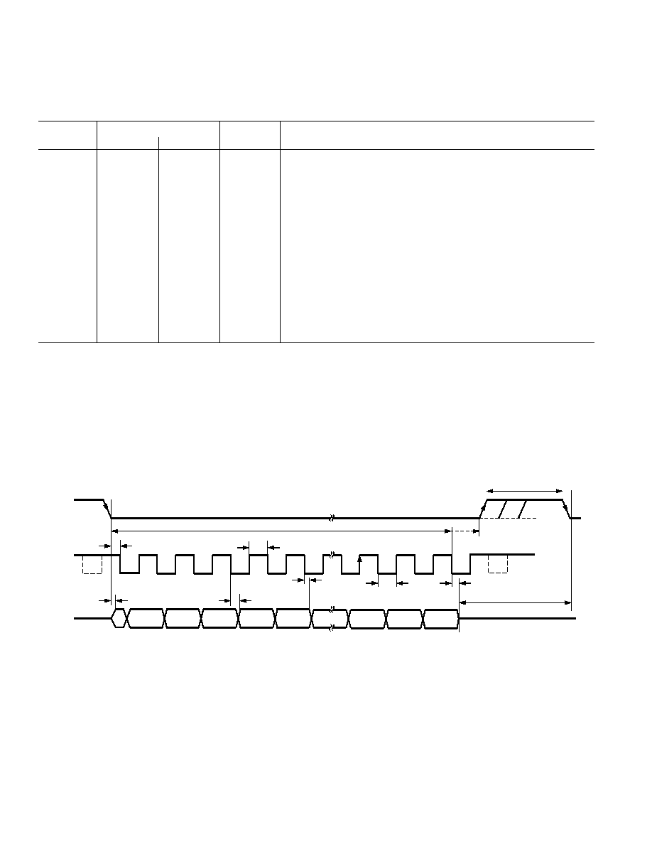
Figure 1. Serial Interface Timing Diagram
TIMING SPECIFICATIONS1, 2 (V
DD = 2.7 V to 3.3 V, fSCLK = 15 MHz, fS = 833 kSPS, VREF = 1.25 V; VDD = 4.75 V to 5.25 V,
fSCLK = 18 MHz, fS = 1 MSPS, VREF = 2.5 V; VCM
3 = V
REF; TA = TMIN to TMAX, unless otherwise noted.)
Rev. A
相关PDF资料 |
PDF描述 |
|---|---|
| VI-B2R-EY | CONVERTER MOD DC/DC 7.5V 50W |
| VI-B1B-EY | CONVERTER MOD DC/DC 95V 50W |
| 0210490922 | CABLE JUMPER 1.25MM .051M 23POS |
| ECA14DCBT | CONN EDGECARD 28POS R/A .125 SLD |
| VE-B1H-EY | CONVERTER MOD DC/DC 52V 50W |
相关代理商/技术参数 |
参数描述 |
|---|---|
| EVAL-AD7451CB | 制造商:Analog Devices 功能描述:DEV TOOLS, PSEUDO DIFFERENTIAL INPUT MSPS 2BIT ADCS - Bulk |
| EVAL-AD7451CBZ | 功能描述:BOARD EVAL FOR AD7451 RoHS:是 类别:编程器,开发系统 >> 评估板 - 模数转换器 (ADC) 系列:- 产品培训模块:Obsolescence Mitigation Program 标准包装:1 系列:- ADC 的数量:1 位数:12 采样率(每秒):94.4k 数据接口:USB 输入范围:±VREF/2 在以下条件下的电源(标准):- 工作温度:-40°C ~ 85°C 已用 IC / 零件:MAX11645 已供物品:板,软件 |
| EVAL-AD7451CBZ3 | 制造商:AD 制造商全称:Analog Devices 功能描述:Pseudo Differential Input, 1 MSPS, 10-/12-Bit ADCs in an 8-Lead SOT-23 |
| EVAL-AD7452CB | 制造商:Analog Devices 功能描述:DEV TOOLS, DIFFERENTIAL INPUT, 555KSPS, 12BIT ADC IN AN 8-LE - Bulk |
| EVAL-AD7452CB3 | 制造商:AD 制造商全称:Analog Devices 功能描述:Differential Input, 555 kSPS 12-Bit ADC in an 8-Lead SOT-23 |
发布紧急采购,3分钟左右您将得到回复。