- 您现在的位置:买卖IC网 > PDF目录17053 > EVAL-AD7450CBZ (Analog Devices Inc)BOARD EVALUATION FOR AD7450 PDF资料下载
参数资料
| 型号: | EVAL-AD7450CBZ |
| 厂商: | Analog Devices Inc |
| 文件页数: | 4/22页 |
| 文件大小: | 0K |
| 描述: | BOARD EVALUATION FOR AD7450 |
| 标准包装: | 1 |
| ADC 的数量: | 1 |
| 位数: | 12 |
| 采样率(每秒): | 1M |
| 数据接口: | DSP,MICROWIRE?,QSPI?,串行,SPI? |
| 输入范围: | ±VREF/2 |
| 在以下条件下的电源(标准): | 9mW @ 1MSPS |
| 工作温度: | -40°C ~ 85°C |
| 已用 IC / 零件: | AD7450 |
| 已供物品: | 板,CD |
| 相关产品: | AD7450BRZ-ND - IC ADC 12BIT DIFF IN 1MSPS 8SOIC AD7450BRMZ-ND - IC ADC 12BIT DIFF IN 1MSPS 8MSOP AD7450ARMZ-ND - IC ADC 12BIT DIFF IN 1MSPS 8MSOP AD7450ABRMZ-ND - IC ADC 12BIT DIFF IN 1MSPS 8MSOP AD7450ARZ-REEL7-ND - IC ADC 12BIT DIFF IN 1MSPS 8SOIC AD7450ARMZ-REEL7-ND - IC ADC 12BIT DIFF IN 1MSPS 8MSOP AD7450ABRTZ-REEL7TR-ND - IC ADC 12BIT DIFF 1MSPS SOT23-8 AD7450ARZ-REEL-ND - IC ADC 12BIT DIFF IN 1MSPS 8SOIC AD7450ARZ-ND - IC ADC 12BIT DIFF-IN 1MSPS 8SOIC AD7450ABRT-R2CT-ND - IC ADC 12BIT W/DIFF INP SOT-23-8 更多... |
–12–
AD7450
REFERENCE = 1.25V
1.25V p-p
COMMON-MODE (CM)
CMMIN = 0.625V
CMMAX = 4.42V
REFERENCE = 2.5V
2.5V p-p
COMMON-MODE (CM)
CMMIN = 1.25V
CMMAX = 3.75V
VIN–
VIN
VIN–
VIN
Figure 10. Examples of the Analog Inputs to VIN+
and VIN– for Different Values of VREF for VDD = 5 V
Analog Input Structure
Figure 11 shows the equivalent circuit of the analog input struc-
ture of the AD7450. The four diodes provide ESD protection
for the analog inputs. Care must be taken to ensure that the
analog input signals never exceed the supply rails by more than
300 mV. This will cause these diodes to become forward biased
and start conducting into the substrate. These diodes can conduct
up to 10 mA without causing irreversible damage to the part.
The capacitors, C1, in Figure 11 are typically 4 pF and can prima-
rily be attributed to pin capacitance. The resistors are lumped
components made up of the ON resistance of the switches. The
value of these resistors is typically about 100
. The capacitors,
C2, are the ADC’s sampling capacitors and have a capacitance
of 16 pF typically.
For ac applications, removing high-frequency components from
the analog input signal is recommended by the use of an RC
low-pass filter on the relevant analog input pins. In applications
where harmonic distortion and signal-to-noise ratio are critical,
the analog input should be driven from a low impedance source.
Large source impedances will significantly affect the ac perfor-
mance of the ADC. This may necessitate the use of an input
buffer amplifier. The choice of the op amp will be a function of
the particular application.
VDD
C1
D
VIN+
R1
C2
VIN–
R1
C2
VDD
D
C1
Figure 11. Equivalent Analog Input Circuit
Conversion Phase—Switches Open
Track Phase—Switches Closed
When no amplifier is used to drive the analog input, the source
impedance should be limited to values lower than 1 k
. The
maximum source impedance will depend on the amount of
total harmonic distortion (THD) that can be tolerated. The THD
will increase as the source impedance increases and the perfor-
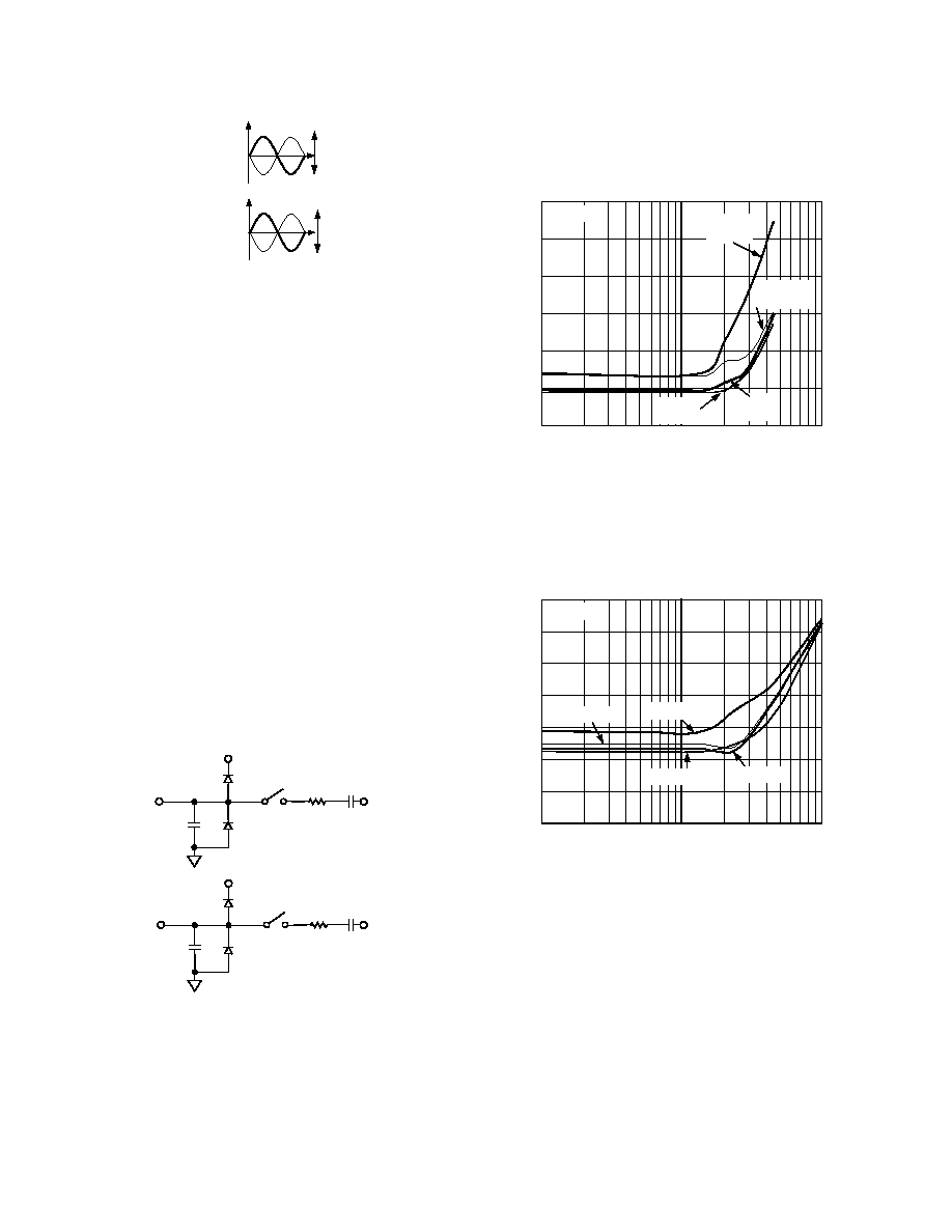
mance will degrade. Figure 12 shows a graph of the THD versus
the analog input signal frequency for different source impedances.
INPUT FREQUENCY – kHz
–74
–70
–72
–76
–78
–82
–80
10
1000
100
THD
–
dBs
TA = 25 C
VDD = 5V
RIN = 1k
VDD = 3V
RIN = 1k
VDD = 3V
RIN = 100
VDD = 5V
RIN = 100
Figure 12. THD vs. Analog Input Frequency for
Various Source Impedances for VDD = 5 V and 3 V
Figure 13 shows a graph of the THD versus the analog input
frequency for VDD of 5 V
± 5% and 3 V ± 10%, while sampling
at 1 MSPS and 833 kSPS with a SCLK of 18 MHz and
15 MHz, respectively. In this case, the source impedance is 10
.
INPUT FREQUENCY – kHz
–95
–70
–60
–65
–75
–80
–90
–85
10
1000
100
THD
–
dBs
TA = 25 C
VDD = 3.3V
VDD = 2.7V
VDD = 4.75V
VDD = 5.25V
Figure 13. THD vs. Analog Input Frequency for 3 V
± 10% and 5 V ± 5% Supply Voltages
DRIVING DIFFERENTIAL INPUTS
Differential operation requires that VIN+ and VIN– be simulta-
neously driven with two equal signals that are 180
o out of phase.
The common mode must be set up externally and has a range
that is determined by VREF, the power supply, and the particular
amplifier used to drive the analog inputs (see Figures 8 and 9).
Differential modes of operation with either an ac or dc input
provide the best THD performance over a wide frequency range.
Since not all applications have a signal preconditioned for
differential operation, there is often a need to perform single-
ended-to-differential conversion.
Rev. A
相关PDF资料 |
PDF描述 |
|---|---|
| VI-B2R-EY | CONVERTER MOD DC/DC 7.5V 50W |
| VI-B1B-EY | CONVERTER MOD DC/DC 95V 50W |
| 0210490922 | CABLE JUMPER 1.25MM .051M 23POS |
| ECA14DCBT | CONN EDGECARD 28POS R/A .125 SLD |
| VE-B1H-EY | CONVERTER MOD DC/DC 52V 50W |
相关代理商/技术参数 |
参数描述 |
|---|---|
| EVAL-AD7451CB | 制造商:Analog Devices 功能描述:DEV TOOLS, PSEUDO DIFFERENTIAL INPUT MSPS 2BIT ADCS - Bulk |
| EVAL-AD7451CBZ | 功能描述:BOARD EVAL FOR AD7451 RoHS:是 类别:编程器,开发系统 >> 评估板 - 模数转换器 (ADC) 系列:- 产品培训模块:Obsolescence Mitigation Program 标准包装:1 系列:- ADC 的数量:1 位数:12 采样率(每秒):94.4k 数据接口:USB 输入范围:±VREF/2 在以下条件下的电源(标准):- 工作温度:-40°C ~ 85°C 已用 IC / 零件:MAX11645 已供物品:板,软件 |
| EVAL-AD7451CBZ3 | 制造商:AD 制造商全称:Analog Devices 功能描述:Pseudo Differential Input, 1 MSPS, 10-/12-Bit ADCs in an 8-Lead SOT-23 |
| EVAL-AD7452CB | 制造商:Analog Devices 功能描述:DEV TOOLS, DIFFERENTIAL INPUT, 555KSPS, 12BIT ADC IN AN 8-LE - Bulk |
| EVAL-AD7452CB3 | 制造商:AD 制造商全称:Analog Devices 功能描述:Differential Input, 555 kSPS 12-Bit ADC in an 8-Lead SOT-23 |
发布紧急采购,3分钟左右您将得到回复。