- 您现在的位置:买卖IC网 > PDF目录17053 > EVAL-AD7476ACBZ (Analog Devices Inc)BOARD EVALUATION FOR AD7476A PDF资料下载
参数资料
| 型号: | EVAL-AD7476ACBZ |
| 厂商: | Analog Devices Inc |
| 文件页数: | 18/29页 |
| 文件大小: | 0K |
| 描述: | BOARD EVALUATION FOR AD7476A |
| 标准包装: | 1 |
| ADC 的数量: | 1 |
| 位数: | 12 |
| 采样率(每秒): | 1M |
| 数据接口: | 串行 |
| 输入范围: | 0 ~ 5.25 V |
| 在以下条件下的电源(标准): | 17.5mW @ 1MSPS,5 V |
| 工作温度: | -40°C ~ 85°C |
| 已用 IC / 零件: | AD7476A |
| 已供物品: | 板,CD |
| 相关产品: | AD7476ARTZ-500RL7DKR-ND - IC ADC 12BIT 1MSPS SOT-23-6 AD7476ABKSZREELDKR-ND - IC ADC 12BIT 1MSPS SC70-6 AD7476BRTZ-R2TR-ND - IC ADC 12BIT 1MSPS SOT23-6 AD7476ARTZ-REEL7-ND - IC ADC 12BIT 1MSPS LP SOT23-6 AD7476ABKSZ-500RL7-ND - IC ADC 12BIT 1MSPS LP SC70-6 AD7476AAKSZ-REEL7-ND - IC ADC 12BIT 1MSPS LP SC70-6 AD7476AAKSZ-500RL7TR-ND - IC ADC 12BIT 1MSPS LP SC70-6 AD7476AYRMZ-REEL7-ND - IC ADC 12BIT 1MSPS LP 8MSOP AD7476AAKSZ-REEL-ND - IC ADC 12BIT 1MSPS LP SC70-6 AD7476ARTZ-500RL7CT-ND - IC ADC 12BIT 1MSPS SOT-23-6 更多... |
第1页第2页第3页第4页第5页第6页第7页第8页第9页第10页第11页第12页第13页第14页第15页第16页第17页当前第18页第19页第20页第21页第22页第23页第24页第25页第26页第27页第28页第29页
AD7476A/AD7477A/AD7478A
Rev. F | Page 24 of 28
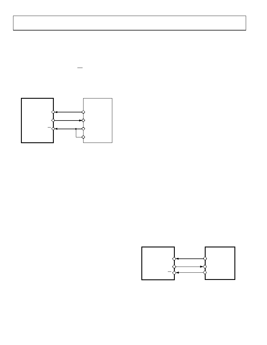
To implement the power-down mode, set SLEN to 0111 to issue
an 8-bit SCLK burst. The connection diagram is shown in
Figure 29. The ADSP-218x has the TFS and RFS of the SPORT
tied together, with TFS set as an output and RFS set as an input.
The DSP operates in alternate framing mode, and the SPORT
control register is set up as described. The frame synchronization
signal generated on the TFS is tied to CS, and, as with all signal
processing applications, equidistant sampling is necessary.
However, in this example, the timer interrupt is used to control
the sampling rate of the ADC and, under certain conditions,
equidistant sampling may not be achieved.
AD7476A/
AD7477A/
AD7478A1
SCLK
SDATA
CS
SCLK
DR
RFS
TFS
ADSP-218x1
1ADDITIONAL PINS OMITTED FOR CLARITY.
02930-029
Figure 29. Interfacing to the ADSP-218x
The timer registers, for example, are loaded with a value that
provides an interrupt at the required sample interval. When an
interrupt is received, a value is transmitted with TFS/DT (ADC
control word). The TFS controls the RFS and, thus, the reading
of data. The frequency of the serial clock is set in the SCLKDIV
register. When the instruction to transmit with TFS is given,
that is, TX0 = AX0, the state of the SCLK is checked. The DSP
waits until the SCLK has gone high, low, and high before
transmission starts. If the timer and SCLK values are chosen
such that the instruction to transmit occurs on or near the
rising edge of SCLK, the data can be transmitted or it can wait
until the next clock edge. For example, the ADSP-2111 has a
master clock frequency of 16 MHz. If the SCLKDIV register is
loaded with the Value 3, an SCLK of 2 MHz is obtained and
eight master clock periods will elapse for every one SCLK
period. If the timer registers are loaded with the Value 803,
100.5 SCLKs occur between interrupts and, subsequently,
between transmit instructions. This situation results in
nonequidistant sampling as the transmit instruction is
occurring on an SCLK edge. If the number of SCLKs between
interrupts is a whole integer figure of N, equidistant sampling is
implemented by the DSP.
AD7476A/AD7477A/AD7478A TO DSP563xx
INTERFACE
The connection diagram in Figure 30 shows how the
AD7476A/AD7477A/AD7478A can be connected to the SSI
(synchronous serial interface) of the DSP563xx family of DSPs
from Motorola. The SSI is operated in synchronous and normal
mode (SYN 1 = and MOD = 0 in Control Register B, CRB) with
internally generated word length frame sync for both Tx and Rx
(Bit FSL1 = 0 and Bit FSL0 = 0 in CRB). Set the word length in
Control Register A (CRA) to 16 by setting Bit WL2 = 0, Bit
WL1 = 1, and Bit WL0 = 0 for the AD7476A. The word length
for the AD7478A can be set to 12 bits (WL2 = 0, WL1 = 0, and
WL0 = 1). This DSP does not offer the option for a 14-bit word
length, so the AD7477A word length is set up to 16 bits, the
same as the AD7476A. For the AD7477A, the conversion process
uses 16 SCLK cycles, with the last two clock periods clocking out
two trailing zeros to fill the 16-bit word.
To implement the power-down mode on the AD7476A/AD7477A/
AD7478A, the word length can be changed to eight bits by setting
Bit WL2 = 0, Bit WL1 = 0, and Bit WL0 = 0 in CRA. The FSP
bit in the CRB register can be set to 1, meaning the frame goes
low and a conversion starts. Likewise, by means of the Bit SCD2,
Bit SCKD, and Bit SHFD in the CRB register, it establishes that
Pin SC2 (the frame sync signal) and Pin SCK in the serial port
are configured as outputs and the MSB is shifted first.
In summary:
MOD = 0
SYN = 1
WL2, WL1, and WL0 depend on the word length
FSL1 = 0 and FSL0 = 0
FSP = 1, negative frame sync
SCD2 = 1
SCKD = 1
SHFD = 0
Note that for signal processing applications, it is imperative that
the frame synchronization signal from the DSP563xx provide
equidistant sampling.
AD7476A/
AD7477A
AD7478A1
SDATA
SCLK
CS
DSP563xx1
SCK
SRD
SC2
1ADDITIONAL PINS OMITTED FOR CLARITY.
02930-030
Figure 30. Interfacing to the DSP563xx
相关PDF资料 |
PDF描述 |
|---|---|
| 0210490923 | CABLE JUMPER 1.25MM .051M 23POS |
| EVAL-AD7450CBZ | BOARD EVALUATION FOR AD7450 |
| VI-B2R-EY | CONVERTER MOD DC/DC 7.5V 50W |
| VI-B1B-EY | CONVERTER MOD DC/DC 95V 50W |
| 0210490922 | CABLE JUMPER 1.25MM .051M 23POS |
相关代理商/技术参数 |
参数描述 |
|---|---|
| EVAL-AD7476CB | 制造商:Analog Devices 功能描述:Evaluation Board For AD7476 制造商:Analog Devices 功能描述:EVALUATION BOARD I.C. - Bulk |
| EVAL-AD7476CBZ | 功能描述:BOARD EVAL FOR AD7476 RoHS:是 类别:编程器,开发系统 >> 评估板 - 模数转换器 (ADC) 系列:* 产品培训模块:Obsolescence Mitigation Program 标准包装:1 系列:- ADC 的数量:1 位数:12 采样率(每秒):94.4k 数据接口:USB 输入范围:±VREF/2 在以下条件下的电源(标准):- 工作温度:-40°C ~ 85°C 已用 IC / 零件:MAX11645 已供物品:板,软件 |
| EVAL-AD7477ACB | 制造商:Analog Devices 功能描述:EVAL BD FOR AD7477A 12-/10-/8BIT ADCS IN 6-LEAD SC70 - Bulk |
| EVAL-AD7477ACB4 | 制造商:AD 制造商全称:Analog Devices 功能描述:2.35 V to 5.25 V, 1 MSPS, 12-/10-/8-Bit ADCs in 6-Lead SC70 |
| EVAL-AD7477CB | 制造商:Analog Devices 功能描述:EVALUATION BOARD I.C. - Bulk |
发布紧急采购,3分钟左右您将得到回复。