- 您现在的位置:买卖IC网 > PDF目录17043 > EVAL-AD7665EDZ (Analog Devices Inc)BOARD EVAL FOR AD76XXEDZ PDF资料下载
参数资料
| 型号: | EVAL-AD7665EDZ |
| 厂商: | Analog Devices Inc |
| 文件页数: | 4/23页 |
| 文件大小: | 0K |
| 描述: | BOARD EVAL FOR AD76XXEDZ |
| 标准包装: | 1 |
| 系列: | * |
REV.
AD7665
–12–
SWA
COMP
SWB
IND
4R
REF
REFGND
LSB
MSB
32,768C
INGND
16,384C
4C
2C
CC
CONTROL
LOGIC
SWITCHES
CONTROL
BUSY
OUTPUT
CODE
INC
4R
INA
R
INB
2R
CNVST
65,536C
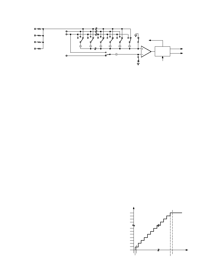
Figure 3. ADC Simplified Schematic
CIRCUIT INFORMATION
The AD7665 is a fast, low power, single-supply, precise 16-bit
analog-to-digital converter (ADC). The AD7665 features different
modes to optimize performances according to the applications.
In Warp Mode, the AD7665 is capable of converting 570,000
samples per second (570 kSPS).
The AD7665 provides the user with an on-chip track-and-hold,
successive approximation ADC that does not exhibit any pipeline
or latency, making it ideal for multiple multiplexed channel
applications.
It is specified to operate with both bipolar and unipolar input
ranges by changing the connection of its input resistive scaler.
The AD7665 can be operated from a single 5 V supply and be
interfaced to either 5 V or 3 V digital logic. It is housed in a
48-lead LQFP package or a 48-lead LFCSP package that com-
bines space savings and flexible configurations as either serial
or parallel interface. The AD7665 is a pin-to-pin compatible
upgrade of the AD7663 and AD7664.
CONVERTER OPERATION
The AD7665 is a successive approximation analog-to-digital
converter based on a charge redistribution DAC. Figure 3 shows
the simplified schematic of the ADC. The input analog signal is
first scaled down and level shifted by the internal input resistive
scaler, which allows both unipolar ranges (0 V to 2.5 V, 0 V to 5 V,
and 0 V to 10 V) and bipolar ranges (±2.5 V, ±5 V, and ±10 V). The
output voltage range of the resistive scaler is always 0 V to 2.5 V.
The capacitive DAC consists of an array of 16 binary weighted
capacitors and an additional “LSB” capacitor. The comparator’s
negative input is connected to a “dummy” capacitor of the same
value as the capacitive DAC array.
During the acquisition phase, the common terminal of the array
tied to the comparator’s positive input is connected to AGND
via SWA. All independent switches are connected to the output
of the resistive scaler. Thus, the capacitor array is used as a
sampling capacitor and acquires the analog signal. Similarly, the
dummy capacitor acquires the analog signal on INGND input.
When the acquisition phase is complete, and the
CNVST input goes
or is LOW, a conversion phase is initiated. When the conversion
phase begins, SWA and SWB are opened first. The capacitor array
and the dummy capacitor are then disconnected from the inputs
and connected to the REFGND input. Therefore, the differential
voltage between the output of the resistive scaler and INGND
captured at the end of the acquisition phase is applied to the
comparator inputs, causing the comparator to become unbalanced.
By switching each element of the capacitor array between REFGND
or REF, the comparator input varies by binary weighted voltage
steps (VREF/2, VREF/4 ... VREF/65,536). The control logic toggles
these switches, starting with the MSB first, in order to bring the
comparator back into a balanced condition. After the completion
of this process, the control logic generates the ADC output code
and brings BUSY output LOW.
Modes of Operation
The AD7665 features three modes of operation, Warp, Normal,
and Impulse. Each of these modes is more suitable for specific
applications.
The Warp Mode allows the fastest conversion rate up to 570 kSPS.
However, in this mode and this mode only, the full specified accu-
racy is guaranteed only when the time between conversion does
not exceed 1 ms. If the time between two consecutive conversions
is longer than 1 ms, for instance, after power-up, the first con-
version result should be ignored. This mode makes the AD7665
ideal for applications where both high accuracy and fast sample
rate are required.
The Normal Mode is the fastest mode (500 kSPS) without any
limitation about the time between conversions. This mode makes
the AD7665 ideal for asynchronous applications such as data
acquisition systems, where both high accuracy and fast sample
rate are required.
The Impulse Mode, the lowest power dissipation mode, allows
power saving between conversions. The maximum throughput in
this mode is 444 kSPS. When operating at 100 SPS, for example,
it typically consumes only 15 W. This feature makes the AD7665
ideal for battery-powered applications.
Transfer Functions
Using the OB/
2C digital input, the AD7665 offers two output
codings: straight binary and twos complement. The ideal transfer
characteristic for the AD7665 is shown in Figure 4 and Table III.
000...000
000...001
000...010
111...101
111...110
111...111
ADC
CODE
–
Straight
Binary
ANALOG INPUT
FS
1.5 LSB
FS
1 LSB
FS
1 LSB
FS
0.5 LSB
Figure 4. ADC Ideal Transfer Function
C
相关PDF资料 |
PDF描述 |
|---|---|
| STD12W-M | WIRE & CABLE MARKERS |
| VE-21V-EY | CONVERTER MOD DC/DC 5.8V 50W |
| VI-21X-EY | CONVERTER MOD DC/DC 5.2V 50W |
| REC5-0505SRW/H6/C | CONV DC/DC 5W 4.5-9VIN 05VOUT |
| STD12W-Q | WIRE & CABLE MARKERS |
相关代理商/技术参数 |
参数描述 |
|---|---|
| EVAL-AD7666CBZ | 功能描述:BOARD EVALUATION FOR AD7666 RoHS:是 类别:编程器,开发系统 >> 评估板 - 模数转换器 (ADC) 系列:PulSAR® 产品培训模块:Obsolescence Mitigation Program 标准包装:1 系列:- ADC 的数量:1 位数:12 采样率(每秒):94.4k 数据接口:USB 输入范围:±VREF/2 在以下条件下的电源(标准):- 工作温度:-40°C ~ 85°C 已用 IC / 零件:MAX11645 已供物品:板,软件 |
| EVAL-AD7667CB | 制造商:Analog Devices 功能描述: |
| EVAL-AD7667CBZ | 功能描述:BOARD EVALUATION FOR AD7667 RoHS:是 类别:编程器,开发系统 >> 评估板 - 模数转换器 (ADC) 系列:PulSAR® 产品培训模块:Obsolescence Mitigation Program 标准包装:1 系列:- ADC 的数量:1 位数:12 采样率(每秒):94.4k 数据接口:USB 输入范围:±VREF/2 在以下条件下的电源(标准):- 工作温度:-40°C ~ 85°C 已用 IC / 零件:MAX11645 已供物品:板,软件 |
| EVAL-AD7668CB | 制造商:AD 制造商全称:Analog Devices 功能描述:Evaluation Board AD766X/AD767X |
| EVAL-AD766XCB | 制造商:AD 制造商全称:Analog Devices 功能描述:Evaluation Board AD766X/AD767X |
发布紧急采购,3分钟左右您将得到回复。