- 您现在的位置:买卖IC网 > PDF目录17043 > EVAL-AD7665EDZ (Analog Devices Inc)BOARD EVAL FOR AD76XXEDZ PDF资料下载
参数资料
| 型号: | EVAL-AD7665EDZ |
| 厂商: | Analog Devices Inc |
| 文件页数: | 6/23页 |
| 文件大小: | 0K |
| 描述: | BOARD EVAL FOR AD76XXEDZ |
| 标准包装: | 1 |
| 系列: | * |
REV.
AD7665
–14–
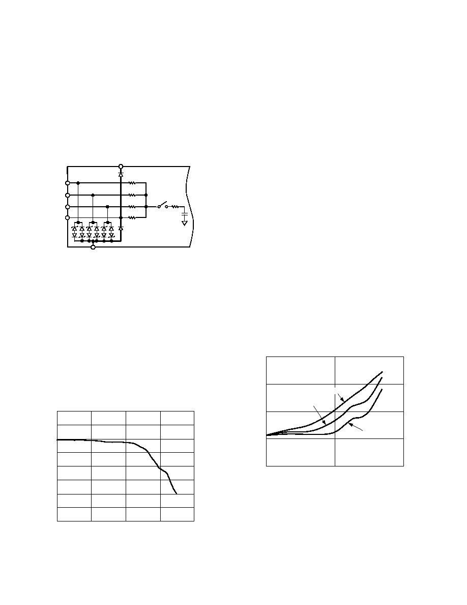
Analog Inputs
The AD7665 is specified to operate with six full-scale analog input
ranges. Connections required for each of the four analog inputs,
IND, INC, INB, and INA, and the resulting full-scale ranges are
shown in Table I. The typical input impedance for each analog
input range is also shown.
Figure 6 shows a simplified analog input section of the AD7665.
The four resistors connected to the four analog inputs form a
resistive scaler that scales down and shifts the analog input range
to a common input range of 0 V to 2.5 V at the input of the
switched capacitive ADC.
INC
INB
INA
4R
2R
R
IND
4R
AGND
AVDD
R1
CS
R = 1.28k
Figure 6. Simplified Analog Input
By connecting the four inputs INA, INB, INC, and IND to the
input signal itself, the ground, or a 2.5 V reference, other analog
input ranges can be obtained.
The diodes shown in Figure 6 provide ESD protection for the
four analog inputs. The inputs INB, INC, and IND have a high
voltage protection (–11 V to +30 V) to allow a wide input voltage
range. Care must be taken to ensure that the analog input signal
never exceeds the absolute ratings on these inputs, including
INA (0 V to 5 V). This will cause these diodes to become forward-
biased and start conducting current. These diodes can handle a
forward-biased current of 120 mA maximum. For instance, when
using the 0 V to 2.5 V input range, these conditions could eventu-
ally occur on the input INA when the input buffer’s (U1) supplies
are different from AVDD. In such cases, an input buffer with a
short circuit current limitation can be used to protect the part.
75
70
65
60
55
50
45
40
35
1
10
100
1000
10000
CMRR
–
dB
FREQUENCY – kHz
Figure 7. Analog Input CMRR vs. Frequency
This analog input structure allows the sampling of the differential
signal between the output of the resistive scaler and INGND.
Unlike other converters, the INGND input is sampled at the same
time as the inputs. By using this differential input, small signals
common to both inputs are rejected as shown in Figure 7, which
represents the typical CMRR over frequency. For instance, by using
INGND to sense a remote signal ground, the difference of ground
potentials between the sensor and the local ADC ground is eliminated.
During the acquisition phase for ac signals, the AD7665 behaves
like a one-pole RC filter consisting of the equivalent resistance
of the resistive scaler R/2 in series with R1 and CS. The resistor
R1 is typically 100
W and is a lumped component made up of
some serial resistors and the on resistance of the switches. The
capacitor CS is typically 60 pF and is mainly the ADC sampling
capacitor. This one-pole filter with a typical –3 dB cutoff frequency
of 3.6 MHz reduces undesirable aliasing effects and limits the
noise coming from the inputs.
Except when using the 0 V to 2.5 V analog input voltage range, the
AD7665 has to be driven by a very low impedance source to avoid
gain errors. That can be done by using a driver amplifier whose
choice is eased by the primarily resistive analog input circuitry of
the AD7665.
When using the 0 V to 2.5 V analog input voltage range, the input
impedance of the AD7665 is very high so the AD7665 can be
driven directly by a low impedance source without gain error.
That allows, as shown in Figure 5, putting an external one-pole
RC filter between the output of the amplifier output and the ADC
analog inputs to even further improve the noise filtering done by
the AD7665 analog input circuit. However, the source impedance
has to be kept low because it affects the ac performances, especially
the total harmonic distortion (THD). The maximum source
impedance depends on the amount of total THD that can be
tolerated. The THD degradation is a function of the source imped-
ance and the maximum input frequency as shown in Figure 8.
FREQUENCY – kHz
–110
0
100
THD
–100
–90
–80
–70
1000
R = 50
R = 11
R = 100
Figure 8. THD vs. Analog Input Frequency and Input
Resistance (0 V to 2.5 V Only)
C
相关PDF资料 |
PDF描述 |
|---|---|
| STD12W-M | WIRE & CABLE MARKERS |
| VE-21V-EY | CONVERTER MOD DC/DC 5.8V 50W |
| VI-21X-EY | CONVERTER MOD DC/DC 5.2V 50W |
| REC5-0505SRW/H6/C | CONV DC/DC 5W 4.5-9VIN 05VOUT |
| STD12W-Q | WIRE & CABLE MARKERS |
相关代理商/技术参数 |
参数描述 |
|---|---|
| EVAL-AD7666CBZ | 功能描述:BOARD EVALUATION FOR AD7666 RoHS:是 类别:编程器,开发系统 >> 评估板 - 模数转换器 (ADC) 系列:PulSAR® 产品培训模块:Obsolescence Mitigation Program 标准包装:1 系列:- ADC 的数量:1 位数:12 采样率(每秒):94.4k 数据接口:USB 输入范围:±VREF/2 在以下条件下的电源(标准):- 工作温度:-40°C ~ 85°C 已用 IC / 零件:MAX11645 已供物品:板,软件 |
| EVAL-AD7667CB | 制造商:Analog Devices 功能描述: |
| EVAL-AD7667CBZ | 功能描述:BOARD EVALUATION FOR AD7667 RoHS:是 类别:编程器,开发系统 >> 评估板 - 模数转换器 (ADC) 系列:PulSAR® 产品培训模块:Obsolescence Mitigation Program 标准包装:1 系列:- ADC 的数量:1 位数:12 采样率(每秒):94.4k 数据接口:USB 输入范围:±VREF/2 在以下条件下的电源(标准):- 工作温度:-40°C ~ 85°C 已用 IC / 零件:MAX11645 已供物品:板,软件 |
| EVAL-AD7668CB | 制造商:AD 制造商全称:Analog Devices 功能描述:Evaluation Board AD766X/AD767X |
| EVAL-AD766XCB | 制造商:AD 制造商全称:Analog Devices 功能描述:Evaluation Board AD766X/AD767X |
发布紧急采购,3分钟左右您将得到回复。