- 您现在的位置:买卖IC网 > PDF目录17032 > EVAL-AD7674CBZ (Analog Devices Inc)BOARD EVALUATION FOR AD7674 PDF资料下载
参数资料
| 型号: | EVAL-AD7674CBZ |
| 厂商: | Analog Devices Inc |
| 文件页数: | 8/28页 |
| 文件大小: | 0K |
| 描述: | BOARD EVALUATION FOR AD7674 |
| 产品培训模块: | ADC Applications ADC Architectures ADC DC/AC Performance |
| 标准包装: | 1 |
| 系列: | PulSAR® |
| ADC 的数量: | 1 |
| 位数: | 18 |
| 采样率(每秒): | 800k |
| 数据接口: | 串行,并联 |
| 输入范围: | 0 ~ 5 V |
| 在以下条件下的电源(标准): | 126mW @ 800kSPS |
| 工作温度: | -40°C ~ 85°C |
| 已用 IC / 零件: | AD7674 |
| 已供物品: | 板 |
| 相关产品: | AD7674ACPZ-ND - IC ADC 18BIT SAR 5V 48LFCSP AD7674ACPZRL-ND - IC ADC 18BIT SAR 5V 48LFCSP AD7674ASTZ-ND - IC ADC 18BIT 800KSPS 48-LQFP AD7674ASTZRL-ND - IC ADC 18BIT 800KSPS 48-LQFP T/R |
第1页第2页第3页第4页第5页第6页第7页当前第8页第9页第10页第11页第12页第13页第14页第15页第16页第17页第18页第19页第20页第21页第22页第23页第24页第25页第26页第27页第28页
AD7674
Rev. A | Page 16 of 28
CIRCUIT INFORMATION
IN+
REF
REFGND
IN–
MSB
4C
2C
C
LSB
SW+
SWITCHES
CONTROL
262,144C 131,072C
MSB
4C
2C
C
LSB
SW–
BUSY
OUTPUT
CODE
CNVST
CONTROL
LOGIC
COMP
262,144C 131,072C
03083–0–025
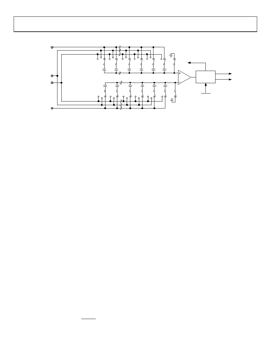
Figure 25. ADC Simplified Schematic
The AD7674 is a very fast, low power, single-supply, precise
18-bit analog-to-digital converter (ADC) using successive
approximation architecture.
The AD7674’s linearity and dynamic range are similar to or
better than many Σ-Δ ADCs. With the advantages of its
successive architecture, which ease multiplexing and reduce
power with throughput, it can be advantageous in applications
that normally use Σ-Δ ADCs.
The AD7674 features different modes to optimize performance
according to the applications. In Warp mode, the AD7674 is
capable of converting 800,000 samples per second (800 kSPS).
The AD7674 provides the user with an on-chip track/hold,
successive approximation ADC that does not exhibit any
pipeline or latency, making it ideal for multiple multiplexed
channel applications.
The AD7674 can be operated from a single 5 V supply and can
be interfaced to either 5 V or 3 V digital logic. It is housed in a
48-lead LQFP, or a tiny 48-lead LFCSP package that offers space
savings and allows for flexible configurations as either a serial
or parallel interface. The AD7674 is a pin-to-pin compatible
upgrade of the AD7676, AD7678, and AD7679.
CONVERTER OPERATION
The AD7674 is a successive approximation ADC based on a
charge redistribution DAC. Figure 25 shows the simplified
schematic of the ADC. The capacitive DAC consists of two
identical arrays of 18 binary weighted capacitors that are
connected to the two comparator inputs.
During the acquisition phase, terminals of the array tied to the
comparator’s input are connected to AGND via SW+ and SW–.
All independent switches are connected to the analog inputs.
Thus, the capacitor arrays are used as sampling capacitors and
acquire the analog signal on the IN+ and IN– inputs. When the
acquisition phase is complete and the CNVST input goes low, a
conversion phase is initiated. When the conversion phase
begins, SW+ and SW– are opened first. The two capacitor
arrays are then disconnected from the inputs and connected to
the REFGND input. Therefore, the differential voltage between
the IN+ and IN– inputs captured at the end of the acquisition
phase is applied to the comparator inputs, causing the
comparator to become unbalanced. By switching each element
of the capacitor array between REFGND and REF, the
comparator input varies by binary weighted voltage steps
(VREF/2, VREF/4, ... VREF/262144). The control logic toggles these
switches, starting with the MSB first, to bring the comparator
back into a balanced condition. After completing this process,
the control logic generates the ADC output code and brings the
BUSY output low.
Modes of Operation
The AD7674 features three modes of operation: Warp, Normal,
and Impulse. Each mode is more suited for specific applications.
Warp mode allows conversion rates up to 800 kSPS. However,
in this mode and this mode only, the full specified accuracy is
guaranteed only when the time between conversions does not
exceed 1 ms. If the time between two consecutive conversions is
longer than 1 ms (e.g., after power-up), the first conversion
result should be ignored. This mode makes the AD7674 ideal
for applications where a fast sample rate is required.
Normal mode is the fastest mode (666 kSPS) without any
limitation on the time between conversions. This mode makes
the AD7674 ideal for asynchronous applications such as data
acquisition systems, where both high accuracy and fast sample
rate are required.
Impulse mode, the lowest power dissipation mode, allows
power saving between conversions. The maximum throughput
in this mode is 570 kSPS. When operating at 1 kSPS, for
example, it typically consumes only 136 μW. This feature makes
the AD7674 ideal for battery-powered applications.
相关PDF资料 |
PDF描述 |
|---|---|
| GEM31DCAD | CONN EDGECARD 62POS R/A .156 SLD |
| GCM25DCAD | CONN EDGECARD 50POS R/A .156 SLD |
| MIC2019A-1YM6 TR | IC POWER SWITCH 1.0A SOT23-6 |
| CB2012T1R0M | INDUCTOR POWER 1.0UH 900MA 0805 |
| ADR430ARZ-REEL7 | IC VREF SERIES PREC 2.048V 8SOIC |
相关代理商/技术参数 |
参数描述 |
|---|---|
| EVAL-AD7674EDZ | 功能描述:BOARD EVAL FOR AD7674 RoHS:是 类别:编程器,开发系统 >> 评估板 - 模数转换器 (ADC) 系列:* 产品培训模块:Obsolescence Mitigation Program 标准包装:1 系列:- ADC 的数量:1 位数:12 采样率(每秒):94.4k 数据接口:USB 输入范围:±VREF/2 在以下条件下的电源(标准):- 工作温度:-40°C ~ 85°C 已用 IC / 零件:MAX11645 已供物品:板,软件 |
| EVAL-AD7675CB | 制造商:AD 制造商全称:Analog Devices 功能描述:Evaluation Board AD766X/AD767X |
| EVAL-AD7675CBZ | 功能描述:BOARD EVALUATION FOR AD7675 RoHS:是 类别:编程器,开发系统 >> 评估板 - 模数转换器 (ADC) 系列:PulSAR® 产品培训模块:Obsolescence Mitigation Program 标准包装:1 系列:- ADC 的数量:1 位数:12 采样率(每秒):94.4k 数据接口:USB 输入范围:±VREF/2 在以下条件下的电源(标准):- 工作温度:-40°C ~ 85°C 已用 IC / 零件:MAX11645 已供物品:板,软件 |
| EVAL-AD7676CB | 制造商:AD 制造商全称:Analog Devices 功能描述:Evaluation Board AD766X/AD767X |
| EVAL-AD7676CBZ | 功能描述:BOARD EVALUATION FOR AD7676 RoHS:是 类别:编程器,开发系统 >> 评估板 - 模数转换器 (ADC) 系列:PulSAR® 产品培训模块:Obsolescence Mitigation Program 标准包装:1 系列:- ADC 的数量:1 位数:12 采样率(每秒):94.4k 数据接口:USB 输入范围:±VREF/2 在以下条件下的电源(标准):- 工作温度:-40°C ~ 85°C 已用 IC / 零件:MAX11645 已供物品:板,软件 |
发布紧急采购,3分钟左右您将得到回复。