- 您现在的位置:买卖IC网 > PDF目录17038 > EVAL-AD7676CBZ (Analog Devices Inc)BOARD EVALUATION FOR AD7676 PDF资料下载
参数资料
| 型号: | EVAL-AD7676CBZ |
| 厂商: | Analog Devices Inc |
| 文件页数: | 8/20页 |
| 文件大小: | 0K |
| 描述: | BOARD EVALUATION FOR AD7676 |
| 标准包装: | 1 |
| 系列: | PulSAR® |
| ADC 的数量: | 1 |
| 位数: | 16 |
| 采样率(每秒): | 500k |
| 数据接口: | 串行,并联 |
| 输入范围: | ±VREF |
| 在以下条件下的电源(标准): | 67mW @ 500kSPS |
| 工作温度: | -40°C ~ 85°C |
| 已用 IC / 零件: | AD7676 |
| 已供物品: | 板 |
| 相关产品: | AD7676ASTZRL-ND - IC ADC 16BIT DIFF INP 48LQFP AD7676ASTZ-ND - IC ADC 16BIT 500KSPS DIFF 48LQFP |
REV. B
AD7676
–16–
In Read-after-Conversion Mode, unlike in other modes, it should
be noted that the signal BUSY returns LOW after the 16 data
bits are pulsed out and not at the end of the conversion phase,
which results in a longer BUSY width.
In Read-during-Conversion Mode, the serial clock and data
toggle at appropriate instances, which minimizes potential feed-
through between digital activity and the critical conversion decisions.
SLAVE SERIAL INTERFACE
External Clock
The AD7676 is configured to accept an externally supplied serial
data clock on the SCLK pin when the EXT/
INT pin is held HIGH.
In this mode, several methods can be used to read the data. The
external serial clock is gated by
CS and the data are output when
both
CS and RD are LOW. Thus, depending on CS, the data can
be read after each conversion or during the following conversion.
The external clock can be either a continuous or discontinuous
clock. A discontinuous clock can be either normally HIGH or
normally LOW when inactive. Figures 19 and 20 show the detailed
timing diagrams of these methods. Usually, because the AD7676
has a longer acquisition phase than the conversion phase, the
data are read immediately after conversion.
While the AD7676 is performing a bit decision, it is important
that voltage transients not occur on digital input/output pins or
degradation of the conversion result could occur. This is particu-
larly important during the second half of the conversion phase
because the AD7676 provides error correction circuitry that can
correct for an improper bit decision made during the first half of
the conversion phase. For this reason, it is recommended that when
an external clock is being provided, it is a discontinuous clock
that is toggling only when BUSY is LOW or, more importantly,
that it does not transition during the latter half of BUSY HIGH.
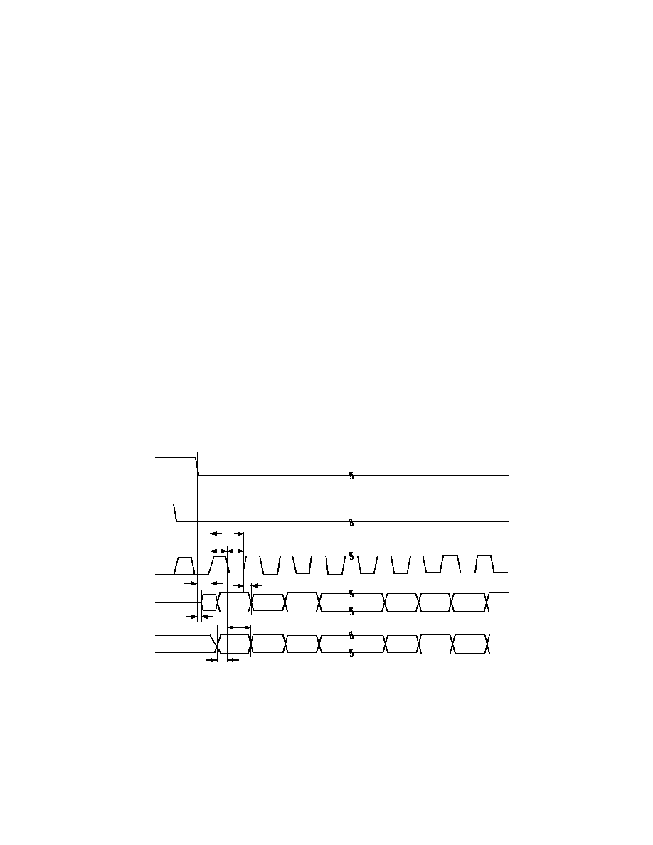
External Discontinuous Clock Data Read after Conversion
This mode is the most recommended of the serial slave modes.
Figure 19 shows the detailed timing diagrams of this method.
After a conversion is complete, indicated by BUSY returning
LOW, the result of this conversion can be read while both
CS and
RD are LOW. The data is shifted out, MSB first, with 16 clock
pulses and is valid on both the rising and falling edges of the clock.
Among the advantages of this method, the conversion perfor-
mance is not degraded because there are no voltage transients
on the digital interface during the conversion process.
Another advantage is to be able to read the data at any speed up to
40 MHz, which accommodates both slow digital host interface
and the fastest serial reading.
Finally, in this mode only, the AD7676 provides a “daisy chain”
feature using the RDC/SDIN input pin for cascading multiple
converters together. This feature is useful for reducing component
count and wiring connections when it is desired as it is, for
instance, in isolated multiconverter applications.
An example of the concatenation of two devices is shown in
Figure 21. Simultaneous sampling is possible by using a common
CNVST signal. It should be noted that the RDC/SDIN input is
latched on the opposite edge of SCLK of the one used to shift
out the data on SDOUT. Thus, the MSB of the “upstream”
converter just follows the LSB of the “downstream” converter
on the next SCLK cycle.
CS
SCLK
SDOUT
D15
D14
D1
D0
D13
X15
X14
X13
X1
X0
Y15
Y14
BUSY
SDIN
INVSCLK = 0
X15
X14
X
12
3
14
15
16
17
18
EXT/
INT = 1
RD = 0
t35
t36 t37
t31
t32
t34
t16
t33
Figure 19. Slave Serial Data Timing for Reading (Read after Conversion)
相关PDF资料 |
PDF描述 |
|---|---|
| LGU2W820MELZ | CAP ALUM 82UF 450V 20% SNAP |
| EBM22DCMN-S288 | CONN EDGECARD 44POS .156 EXTEND |
| MPC8306-SOM | MODULE BOARD FOR MPC830X |
| EVAL-AD7610CBZ | BOARD EVALUATION FOR AD7610 |
| EVAL-AD7651CBZ | BOARD EVALUATION FOR AD7651 |
相关代理商/技术参数 |
参数描述 |
|---|---|
| EVAL-AD7676EDZ | 功能描述:BOARD EVAL FOR AD7676 RoHS:是 类别:编程器,开发系统 >> 评估板 - 模数转换器 (ADC) 系列:PulSAR® 产品培训模块:Obsolescence Mitigation Program 标准包装:1 系列:- ADC 的数量:1 位数:12 采样率(每秒):94.4k 数据接口:USB 输入范围:±VREF/2 在以下条件下的电源(标准):- 工作温度:-40°C ~ 85°C 已用 IC / 零件:MAX11645 已供物品:板,软件 |
| EVAL-AD7677CB | 制造商:AD 制造商全称:Analog Devices 功能描述:Evaluation Board AD766X/AD767X |
| EVAL-AD7677CBZ | 功能描述:BOARD EVALUATION FOR AD7677 RoHS:是 类别:编程器,开发系统 >> 评估板 - 模数转换器 (ADC) 系列:PulSAR® 产品培训模块:Obsolescence Mitigation Program 标准包装:1 系列:- ADC 的数量:1 位数:12 采样率(每秒):94.4k 数据接口:USB 输入范围:±VREF/2 在以下条件下的电源(标准):- 工作温度:-40°C ~ 85°C 已用 IC / 零件:MAX11645 已供物品:板,软件 |
| EVAL-AD7677EDZ | 功能描述:BOARD EVAL FOR AD7677 RoHS:是 类别:编程器,开发系统 >> 评估板 - 模数转换器 (ADC) 系列:* 产品培训模块:Obsolescence Mitigation Program 标准包装:1 系列:- ADC 的数量:1 位数:12 采样率(每秒):94.4k 数据接口:USB 输入范围:±VREF/2 在以下条件下的电源(标准):- 工作温度:-40°C ~ 85°C 已用 IC / 零件:MAX11645 已供物品:板,软件 |
| EVAL-AD7678CB | 功能描述:BOARD EVALUATION FOR AD7678 RoHS:否 类别:编程器,开发系统 >> 评估板 - 模数转换器 (ADC) 系列:PulSAR® 产品培训模块:Obsolescence Mitigation Program 标准包装:1 系列:- ADC 的数量:1 位数:12 采样率(每秒):94.4k 数据接口:USB 输入范围:±VREF/2 在以下条件下的电源(标准):- 工作温度:-40°C ~ 85°C 已用 IC / 零件:MAX11645 已供物品:板,软件 |
发布紧急采购,3分钟左右您将得到回复。