- 您现在的位置:买卖IC网 > PDF目录17040 > EVAL-AD7686CBZ (Analog Devices Inc)BOARD EVALUATION FOR AD7686 PDF资料下载
参数资料
| 型号: | EVAL-AD7686CBZ |
| 厂商: | Analog Devices Inc |
| 文件页数: | 10/28页 |
| 文件大小: | 0K |
| 描述: | BOARD EVALUATION FOR AD7686 |
| 标准包装: | 1 |
| 系列: | PulSAR® |
| ADC 的数量: | 1 |
| 位数: | 16 |
| 采样率(每秒): | 500k |
| 数据接口: | 串行 |
| 输入范围: | ±VREF |
| 在以下条件下的电源(标准): | 15mW @ 500kSPS,5 V |
| 工作温度: | -40°C ~ 85°C |
| 已用 IC / 零件: | AD7686 |
| 已供物品: | 板 |
| 相关产品: | AD7686CCPZRL7TR-ND - IC ADC 16BIT SAR 500KSPS 10LFCSP AD7686CCPZRL-ND - IC ADC 16BIT SAR 500KSPS 10LFCSP AD7686BCPZRL7TR-ND - IC ADC 16BIT 500KSPS 10-LFCSP AD7686BCPZRL-ND - IC ADC 16BIT 500KSPS 10-LFCSP AD7686CRMZ-ND - IC ADC 16BIT 500KSPS 10MSOP AD7686BRMZ-ND - IC ADC 16BIT 500KSPS 10-MSOP AD7686CRMZRL7-ND - IC ADC 16BIT 500KSPS 10MSOP AD7686BRMZRL7-ND - IC ADC 16BIT 500KSPS 10MSOP |
第1页第2页第3页第4页第5页第6页第7页第8页第9页当前第10页第11页第12页第13页第14页第15页第16页第17页第18页第19页第20页第21页第22页第23页第24页第25页第26页第27页第28页
AD7686
Rev. B | Page 18 of 28
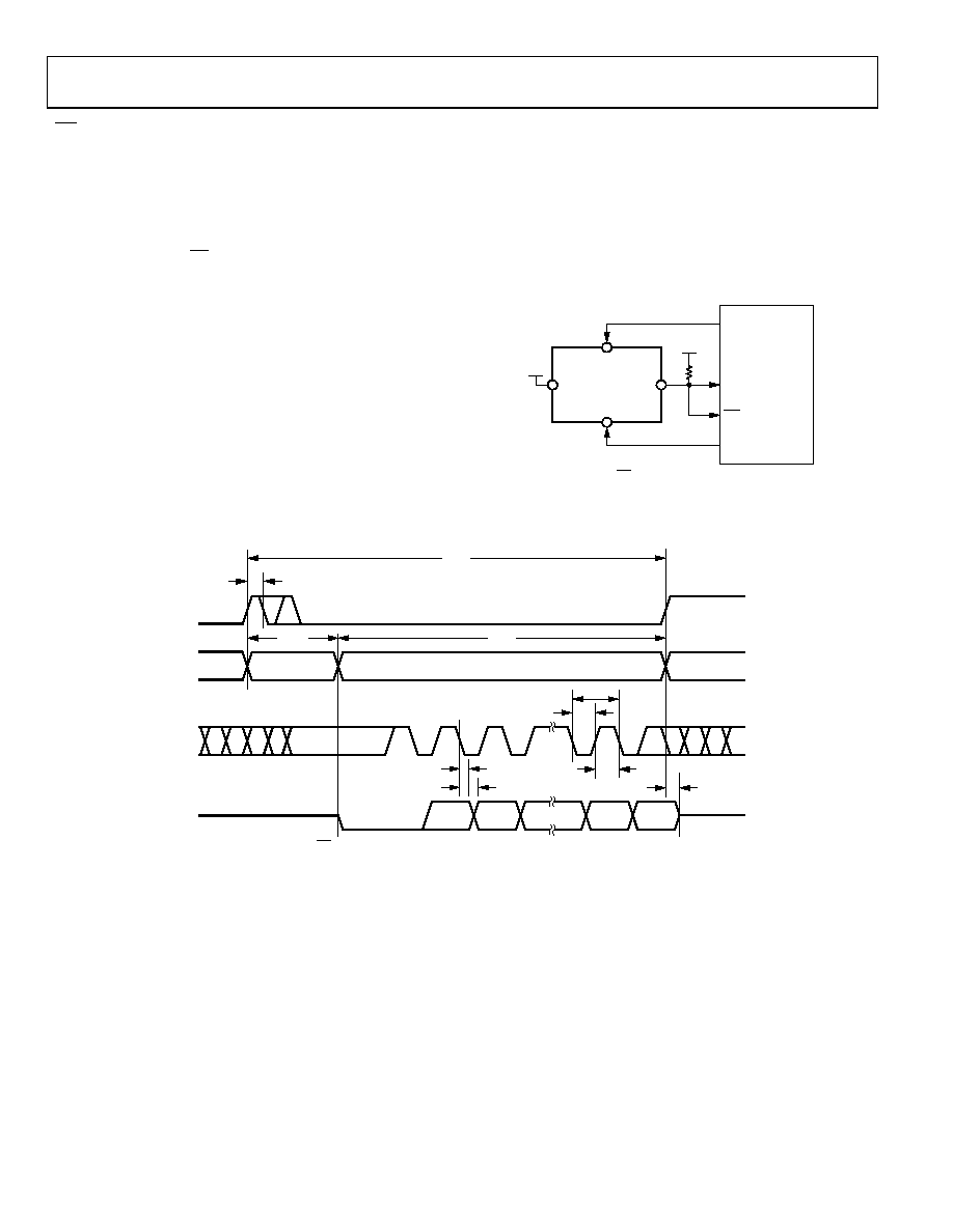
CS MODE 3-WIRE WITH BUSY INDICATOR
This mode is generally used when a single AD7686 is connected
to an SPI-compatible digital host having an interrupt input. The
connection diagram is shown in Figure 35, and the correspond-
ing timing is provided in Figure 36.
With SDI tied to VIO, a rising edge on CNV initiates a
conversion, selects the CS mode, and forces SDO to high
impedance. SDO is maintained in high impedance until the
completion of the conversion, irrespective of the state of CNV.
Prior to the minimum conversion time, CNV can be used to
select other SPI devices, such as analog multiplexers. However,
CNV must be returned low before the minimum conversion
time and held low until the maximum conversion time to
guarantee the generation of the busy signal indicator. When the
conversion is complete, SDO goes from high impedance to low.
With a pull-up on the SDO line, this transition can be used as
an interrupt signal to initiate the data reading controlled by the
digital host. The AD7686 then enters the acquisition phase and
powers down. The data bits are then clocked out, MSB first, by
subsequent SCK falling edges. The data is valid on both SCK edges.
Although the rising edge can be used to capture the data, a
digital host using the SCK falling edge allows a faster reading
rate, provided it has an acceptable hold time. After the optional
17th SCK falling edge or when CNV goes high, whichever
occurs first, SDO returns to high impedance.
If multiple AD7686s are selected at the same time, the SDO
output pin handles this connection without damage or induced
latch-up. Meanwhile, it is recommended to keep this connection as
short as possible to limit extra power dissipation.
DATA IN
IRQ
CLK
CONVERT
VIO
DIGITAL HOST
02
969
-03
6
47k
CNV
SCK
SDO
SDI
VIO
AD7686
Figure 35. CS Mode 3-Wire with Busy Indicator
Connection Diagram (SDI High)
SDO
D15
D14
D1
D0
tDIS
SCK
1
2
3
15
16
17
tSCK
tSCKL
tSCKH
tHSDO
tDSDO
CNV
CONVERSION
ACQUISITION
tCONV
tCYC
tCNVH
tACQ
ACQUISITION
SDI = 1
0
29
69
-03
7
Figure 36. CS Mode 3-Wire with Busy Indicator Serial Interface Timing (SDI High)
相关PDF资料 |
PDF描述 |
|---|---|
| HBC06DRTH-S93 | CONN EDGECARD 12POS DIP .100 SLD |
| MCP355XDV-MS1 | BOARD DEV SENSOR APP MCP355X |
| UPB2D681MRD | CAP ALUM 680UF 200V 20% RADIAL |
| MLG1005S68NJ | INDUCTOR MULTILAYER 68NH 0402 |
| GCC06DRYI-S93 | CONN EDGECARD 12POS DIP .100 SLD |
相关代理商/技术参数 |
参数描述 |
|---|---|
| EVAL-AD7686SDZ | 功能描述:数据转换 IC 开发工具 EVAL BOARD 100Ksps/400Ksps 16 bit I.C RoHS:否 制造商:Texas Instruments 产品:Demonstration Kits 类型:ADC 工具用于评估:ADS130E08 接口类型:SPI 工作电源电压:- 6 V to + 6 V |
| EVAL-AD7687CB | 制造商:Analog Devices 功能描述:EVAL BOARD 16-BIT, 250KSPS DIFFER . I.C. - Bulk |
| EVAL-AD7687CBZ | 功能描述:BOARD EVALUATION FOR AD7687 RoHS:是 类别:编程器,开发系统 >> 评估板 - 模数转换器 (ADC) 系列:PulSAR® 产品培训模块:Obsolescence Mitigation Program 标准包装:1 系列:- ADC 的数量:1 位数:12 采样率(每秒):94.4k 数据接口:USB 输入范围:±VREF/2 在以下条件下的电源(标准):- 工作温度:-40°C ~ 85°C 已用 IC / 零件:MAX11645 已供物品:板,软件 |
| EVAL-AD7687SDZ | 功能描述:BOARD EVAL FOR AD7687 RoHS:是 类别:编程器,开发系统 >> 评估板 - 模数转换器 (ADC) 系列:PulSAR® 产品培训模块:Obsolescence Mitigation Program 标准包装:1 系列:- ADC 的数量:1 位数:12 采样率(每秒):94.4k 数据接口:USB 输入范围:±VREF/2 在以下条件下的电源(标准):- 工作温度:-40°C ~ 85°C 已用 IC / 零件:MAX11645 已供物品:板,软件 |
| EVAL-AD7688CB | 制造商:Analog Devices 功能描述:EVAL BD FOR USE W/ EITHER THE ANLG DEVICES - Bulk |
发布紧急采购,3分钟左右您将得到回复。