- 您现在的位置:买卖IC网 > PDF目录17040 > EVAL-AD7686CBZ (Analog Devices Inc)BOARD EVALUATION FOR AD7686 PDF资料下载
参数资料
| 型号: | EVAL-AD7686CBZ |
| 厂商: | Analog Devices Inc |
| 文件页数: | 26/28页 |
| 文件大小: | 0K |
| 描述: | BOARD EVALUATION FOR AD7686 |
| 标准包装: | 1 |
| 系列: | PulSAR® |
| ADC 的数量: | 1 |
| 位数: | 16 |
| 采样率(每秒): | 500k |
| 数据接口: | 串行 |
| 输入范围: | ±VREF |
| 在以下条件下的电源(标准): | 15mW @ 500kSPS,5 V |
| 工作温度: | -40°C ~ 85°C |
| 已用 IC / 零件: | AD7686 |
| 已供物品: | 板 |
| 相关产品: | AD7686CCPZRL7TR-ND - IC ADC 16BIT SAR 500KSPS 10LFCSP AD7686CCPZRL-ND - IC ADC 16BIT SAR 500KSPS 10LFCSP AD7686BCPZRL7TR-ND - IC ADC 16BIT 500KSPS 10-LFCSP AD7686BCPZRL-ND - IC ADC 16BIT 500KSPS 10-LFCSP AD7686CRMZ-ND - IC ADC 16BIT 500KSPS 10MSOP AD7686BRMZ-ND - IC ADC 16BIT 500KSPS 10-MSOP AD7686CRMZRL7-ND - IC ADC 16BIT 500KSPS 10MSOP AD7686BRMZRL7-ND - IC ADC 16BIT 500KSPS 10MSOP |
第1页第2页第3页第4页第5页第6页第7页第8页第9页第10页第11页第12页第13页第14页第15页第16页第17页第18页第19页第20页第21页第22页第23页第24页第25页当前第26页第27页第28页
AD7686
Rev. B | Page 7 of 28
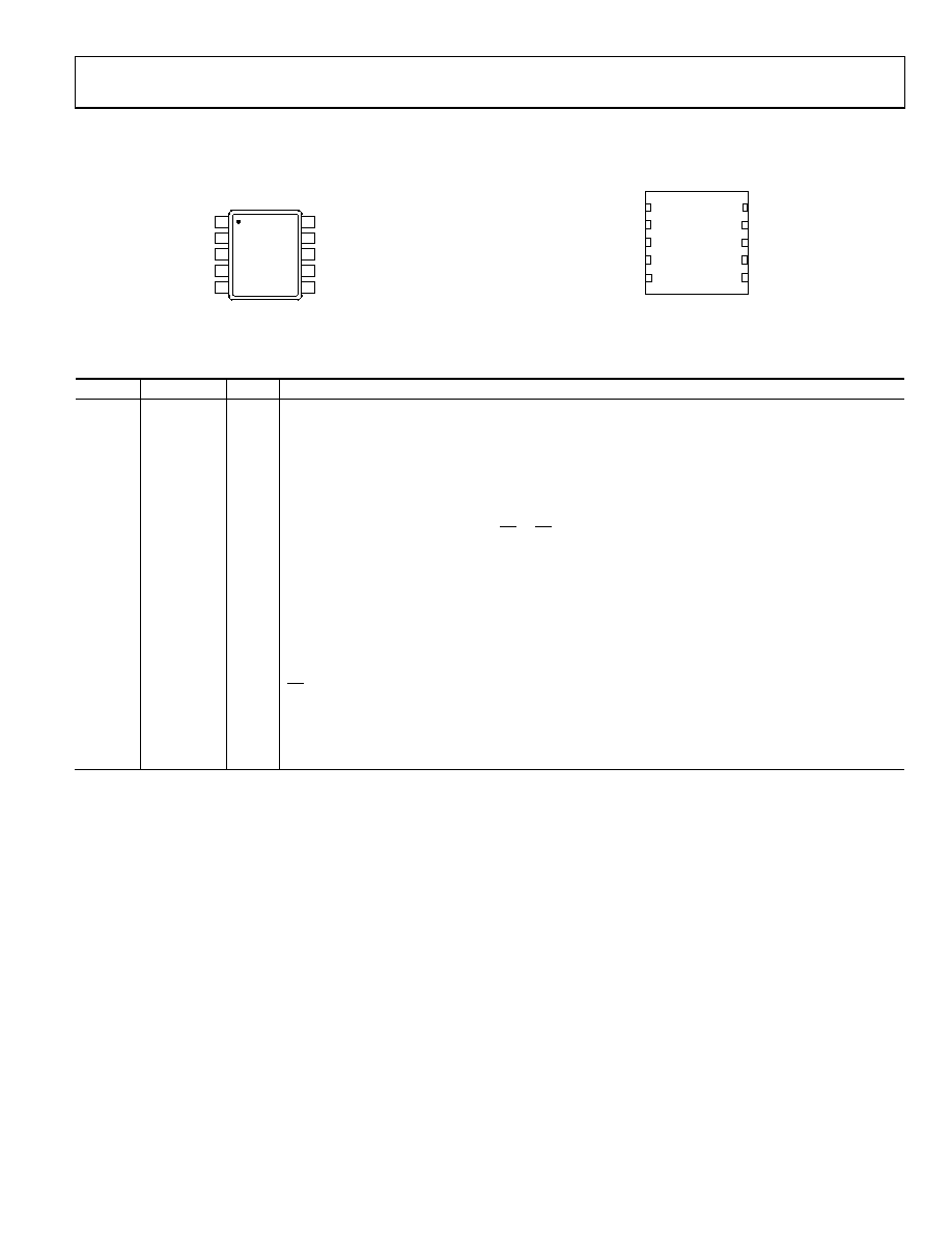
PIN CONFIGURATIONS AND FUNCTION DESCRIPTIONS
02
969
-00
5
REF 1
VDD 2
IN+ 3
IN– 4
GND 5
VIO
10
SDI
9
SCK
8
SDO
7
CNV
6
AD7686
TOP VIEW
(Not to Scale)
Figure 5. 10-Lead MSOP Pin Configuration
02
969
-00
6
1
REF
2
VDD
3
IN+
4
IN–
5
GND
10 VIO
9SDI
8SCK
7SDO
6CNV
TOP VIEW
(Not to Scale)
AD7686
Figure 6. 10-Lead QFN (LFCSP) Pin Configuration
Table 6. Pin Function Descriptions
Pin No.
Mnemonic
Type1
Description
1
REF
AI
Reference Input Voltage. The REF range is from 0.5 V to VDD. It is referred to the GND pin. This pin should
be decoupled closely to the pin with a 10 μF capacitor.
2
VDD
P
Power Supply.
3
IN+
AI
Analog Input. It is referred to IN. The voltage range, that is, the difference between IN+ and IN, is 0 V to VREF.
4
IN
AI
Analog Input Ground Sense. It is connected to the analog ground plane or to a remote sense ground.
5
GND
P
Power Supply Ground.
6
CNV
DI
Convert Input. This input has multiple functions. On its leading edge, it initiates the conversions and
selects the interface mode, chain, or CS. In CS mode, it enables the SDO pin when low. In chain mode,
the data should be read when CNV is high.
7
SDO
DO
Serial Data Output. The conversion result is output on this pin. It is synchronized to SCK.
8
SCK
DI
Serial Data Clock Input. When the part is selected, the conversion result is shifted out by this clock.
9
SDI
DI
Serial Data Input. This input provides multiple features. It selects the interface mode of the ADC as
follows:
Chain mode is selected if SDI is low during the CNV rising edge. In this mode, SDI is used as a data
input to daisy-chain the conversion results of two or more ADCs onto a single SDO line. The digital
data level on SDI is output on SDO with a delay of 16 SCK cycles.
CS mode is selected if SDI is high during the CNV rising edge. In this mode, either SDI or CNV can
enable the serial output signals when low. If SDI or CNV is low when the conversion is completed,
the busy indicator feature is enabled.
10
VIO
P
Input/Output Interface Digital Power. Nominally at the same supply as the host interface (1.8 V, 2.5 V,
3 V, or 5 V).
1AI = analog input, DI = digital input, DO = digital output, and P = power.
相关PDF资料 |
PDF描述 |
|---|---|
| HBC06DRTH-S93 | CONN EDGECARD 12POS DIP .100 SLD |
| MCP355XDV-MS1 | BOARD DEV SENSOR APP MCP355X |
| UPB2D681MRD | CAP ALUM 680UF 200V 20% RADIAL |
| MLG1005S68NJ | INDUCTOR MULTILAYER 68NH 0402 |
| GCC06DRYI-S93 | CONN EDGECARD 12POS DIP .100 SLD |
相关代理商/技术参数 |
参数描述 |
|---|---|
| EVAL-AD7686SDZ | 功能描述:数据转换 IC 开发工具 EVAL BOARD 100Ksps/400Ksps 16 bit I.C RoHS:否 制造商:Texas Instruments 产品:Demonstration Kits 类型:ADC 工具用于评估:ADS130E08 接口类型:SPI 工作电源电压:- 6 V to + 6 V |
| EVAL-AD7687CB | 制造商:Analog Devices 功能描述:EVAL BOARD 16-BIT, 250KSPS DIFFER . I.C. - Bulk |
| EVAL-AD7687CBZ | 功能描述:BOARD EVALUATION FOR AD7687 RoHS:是 类别:编程器,开发系统 >> 评估板 - 模数转换器 (ADC) 系列:PulSAR® 产品培训模块:Obsolescence Mitigation Program 标准包装:1 系列:- ADC 的数量:1 位数:12 采样率(每秒):94.4k 数据接口:USB 输入范围:±VREF/2 在以下条件下的电源(标准):- 工作温度:-40°C ~ 85°C 已用 IC / 零件:MAX11645 已供物品:板,软件 |
| EVAL-AD7687SDZ | 功能描述:BOARD EVAL FOR AD7687 RoHS:是 类别:编程器,开发系统 >> 评估板 - 模数转换器 (ADC) 系列:PulSAR® 产品培训模块:Obsolescence Mitigation Program 标准包装:1 系列:- ADC 的数量:1 位数:12 采样率(每秒):94.4k 数据接口:USB 输入范围:±VREF/2 在以下条件下的电源(标准):- 工作温度:-40°C ~ 85°C 已用 IC / 零件:MAX11645 已供物品:板,软件 |
| EVAL-AD7688CB | 制造商:Analog Devices 功能描述:EVAL BD FOR USE W/ EITHER THE ANLG DEVICES - Bulk |
发布紧急采购,3分钟左右您将得到回复。