- 您现在的位置:买卖IC网 > PDF目录17044 > EVAL-AD7687SDZ (Analog Devices Inc)BOARD EVAL FOR AD7687 PDF资料下载
参数资料
| 型号: | EVAL-AD7687SDZ |
| 厂商: | Analog Devices Inc |
| 文件页数: | 7/28页 |
| 文件大小: | 0K |
| 描述: | BOARD EVAL FOR AD7687 |
| 标准包装: | 1 |
| 系列: | PulSAR® |
| ADC 的数量: | 1 |
| 位数: | 16 |
| 采样率(每秒): | 250k |
| 数据接口: | 串行 |
| 输入范围: | ±VREF |
| 在以下条件下的电源(标准): | 4mW @ 5V,100kSPS |
| 工作温度: | -40°C ~ 85°C |
| 已用 IC / 零件: | AD7687 |
| 已供物品: | 板 |
第1页第2页第3页第4页第5页第6页当前第7页第8页第9页第10页第11页第12页第13页第14页第15页第16页第17页第18页第19页第20页第21页第22页第23页第24页第25页第26页第27页第28页
Data Sheet
AD7687
Rev. B | Page 15 of 28
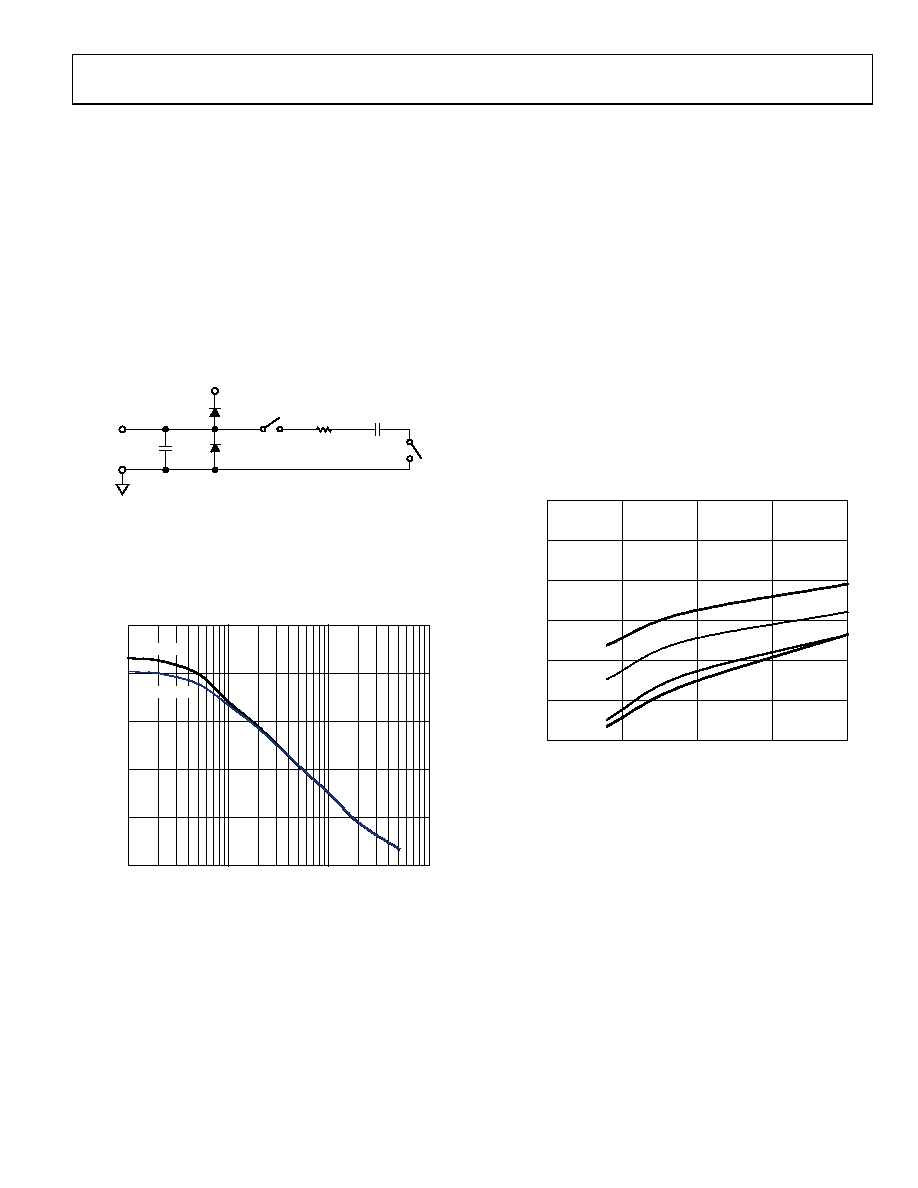
ANALOG INPUT
Figure 28 shows an equivalent circuit of the input structure of
the AD7687.
The two diodes, D1 and D2, provide ESD protection for the
analog inputs IN+ and IN. Care must be taken to ensure that
the analog input signal never exceeds the supply rails by more
than 0.3 V because this causes these diodes to begin to forward-
bias and start conducting current. These diodes can handle a
forward-biased current of 130 mA maximum. For instance,
these conditions could eventually occur when the input buffer’s
(U1) supplies are different from VDD. In such a case, an input
buffer with a short-circuit current limitation can be used to
protect the part.
CIN
RIN
D1
D2
CPIN
IN+
OR IN–
GND
VDD
02972-027
Figure 28. Equivalent Analog Input Circuit
The analog input structure allows the sampling of the true
differential signal between IN+ and IN. By using these
differential inputs, signals common to both inputs are rejected,
as shown in Figure 29, which represents the typical CMRR over
frequency.
FREQUENCY (kHz)
CM
RR
(dB)
90
80
70
60
40
50
1
10
100
1000
02972-
028
VDD = 5V
VDD = 2.5V
Figure 29. Analog Input CMRR vs. Frequency
During the acquisition phase, the impedance of the analog
inputs (IN+ or IN) can be modeled as a parallel combination
of capacitor, CPIN, and the network formed by the series
connection of RIN and CIN. CPIN is primarily the pin capacitance.
RIN is typically 3 kΩ and is a lumped component made up of
some serial resistors and the on resistance of the switches. CIN is
typically 30 pF and is mainly the ADC sampling capacitor.
During the conversion phase, where the switches are opened,
the input impedance is limited to CPIN. RIN and CIN make a
1-pole, low-pass filter that reduces undesirable aliasing effects
and limits the noise.
When the source impedance of the driving circuit is low, the
AD7687 can be driven directly. Large source impedances
significantly affect the ac performance, especially total
harmonic distortion (THD). The dc performances are less
sensitive to the input impedance. The maximum source
impedance depends on the amount of THD that can be
tolerated. The THD degrades as a function of the source
impedance and the maximum input frequency, as shown in
FREQUENCY (kHz)
THD
(dB)
–60
–70
–80
–90
–100
–110
–120
0
25
50
75
100
02972-
029
RS = 250Ω
RS = 100Ω
RS = 50Ω
RS = 33Ω
Figure 30. THD vs. Analog Input Frequency and Source Resistance
相关PDF资料 |
PDF描述 |
|---|---|
| RCM08DRAI | CONN EDGECARD 16POS R/A .156 SLD |
| MIC2076A-1YM | IC SW DISTRIBUTION 2CH 8SOIC |
| 0210490301 | CABLE JUMPER 1.25MM .051M 24POS |
| LGU2G560MELY | CAP ALUM 56UF 400V 20% SNAP |
| ADR420ARZ-REEL7 | IC VREF SERIES PREC 2.048V 8SOIC |
相关代理商/技术参数 |
参数描述 |
|---|---|
| EVAL-AD7688CB | 制造商:Analog Devices 功能描述:EVAL BD FOR USE W/ EITHER THE ANLG DEVICES - Bulk |
| EVAL-AD7688CBZ | 功能描述:BOARD EVAL FOR AD7688 RoHS:是 类别:编程器,开发系统 >> 评估板 - 模数转换器 (ADC) 系列:PulSAR® 产品培训模块:Obsolescence Mitigation Program 标准包装:1 系列:- ADC 的数量:1 位数:12 采样率(每秒):94.4k 数据接口:USB 输入范围:±VREF/2 在以下条件下的电源(标准):- 工作温度:-40°C ~ 85°C 已用 IC / 零件:MAX11645 已供物品:板,软件 |
| EVAL-AD7688SDZ | 功能描述:BOARD EVAL FOR AD7688 RoHS:是 类别:编程器,开发系统 >> 评估板 - 模数转换器 (ADC) 系列:PulSAR® 产品培训模块:Obsolescence Mitigation Program 标准包装:1 系列:- ADC 的数量:1 位数:12 采样率(每秒):94.4k 数据接口:USB 输入范围:±VREF/2 在以下条件下的电源(标准):- 工作温度:-40°C ~ 85°C 已用 IC / 零件:MAX11645 已供物品:板,软件 |
| EVAL-AD7689CBZ | 制造商:Analog Devices 功能描述:EVAL BOARD 8 CH 250KSPS 16BIT ADC IC - Bulk |
| EVAL-AD7689EDZ | 功能描述:BOARD EVAL AD7689 RoHS:是 类别:编程器,开发系统 >> 评估板 - 模数转换器 (ADC) 系列:PulSAR® 产品培训模块:Obsolescence Mitigation Program 标准包装:1 系列:- ADC 的数量:1 位数:12 采样率(每秒):94.4k 数据接口:USB 输入范围:±VREF/2 在以下条件下的电源(标准):- 工作温度:-40°C ~ 85°C 已用 IC / 零件:MAX11645 已供物品:板,软件 |
发布紧急采购,3分钟左右您将得到回复。