- 您现在的位置:买卖IC网 > PDF目录17044 > EVAL-AD7687SDZ (Analog Devices Inc)BOARD EVAL FOR AD7687 PDF资料下载
参数资料
| 型号: | EVAL-AD7687SDZ |
| 厂商: | Analog Devices Inc |
| 文件页数: | 8/28页 |
| 文件大小: | 0K |
| 描述: | BOARD EVAL FOR AD7687 |
| 标准包装: | 1 |
| 系列: | PulSAR® |
| ADC 的数量: | 1 |
| 位数: | 16 |
| 采样率(每秒): | 250k |
| 数据接口: | 串行 |
| 输入范围: | ±VREF |
| 在以下条件下的电源(标准): | 4mW @ 5V,100kSPS |
| 工作温度: | -40°C ~ 85°C |
| 已用 IC / 零件: | AD7687 |
| 已供物品: | 板 |
第1页第2页第3页第4页第5页第6页第7页当前第8页第9页第10页第11页第12页第13页第14页第15页第16页第17页第18页第19页第20页第21页第22页第23页第24页第25页第26页第27页第28页
AD7687
Data Sheet
Rev. B | Page 16 of 28
DRIVER AMPLIFIER CHOICE
Although the AD7687 is easy to drive, the driver amplifier
needs to meet the following requirements:
The noise generated by the driver amplifier needs to be
kept as low as possible in order to preserve the SNR and
transition noise performance of the AD7687. Note that
the AD7687 has a noise much lower than most of the other
16-bit ADCs and, therefore, can be driven by a noisier op
amp while preserving the same or better system perform-
ance. The noise coming from the driver is filtered by the
AD7687 analog input circuit 1-pole, low-pass filter made
by RIN and CIN or by the external filter, if one is used.
Because the typical noise of the AD7687 is 53 μV rms,
the SNR degradation due to the amplifier is
()
+
=
2
3dB
2
π
53
20log
N
LOSS
Ne
f
SNR
where:
f–3dB is the input bandwidth in MHz of the AD7687
(2 MHz) or the cutoff frequency of the input filter, if
one is used.
N is the noise gain of the amplifier (for example, +1 in
buffer configuration).
eN is the equivalent input noise voltage of the op amp,
in nV/√Hz.
For ac applications, the driver should have a THD
performance commensurate with the AD7687. Figure 17
shows the THD vs. frequency that the driver should
exceed.
For multichannel multiplexed applications, the driver
amplifier and the AD7687 analog input circuit must settle a
full-scale step onto the capacitor array at a 16-bit level
(0.0015%, 15 ppm). In the amplifier’s data sheet, settling at
0.1% to 0.01% is more commonly specified. This could
differ significantly from the settling time at a 16-bit level
and should be verified prior to driver selection.
Table 10. Recommended Driver Amplifiers.
Amplifier
Typical Application
Very low noise and high frequency
Low noise and high frequency
Low power, low noise, and low frequency
5 V single-supply, low power
Small, low power and low frequency
High frequency and low power
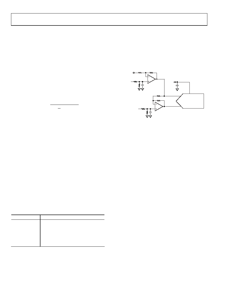
SINGLE-TO-DIFFERENTIAL DRIVER
For applications using a single-ended analog signal, either
bipolar or unipolar, a single-ended-to-differential driver
allows for a differential input into the part (see Figure 31 for
the schematic). When provided a single-ended input signal,
this configuration produces a differential ±VREF with midscale
at VREF/2.
U2
10k
Ω
590
Ω
AD7687
IN+
IN–
REF
U1
ANALOG INPUT
(
±10V, ±5V, ..)
590
Ω
10
μF
100nF
10k
Ω
VREF
590
Ω
100nF
VREF
02972-030
Figure 31. Single-Ended-to-Differential Driver Circuit
VOLTAGE REFERENCE INPUT
The AD7687 voltage reference input, REF, has a dynamic input
impedance and should therefore be driven by a low impedance
source with efficient decoupling between the REF and GND
pins, as explained in the Layout section.
When REF is driven by a very low impedance source, for
10 μF (X5R, 0805 size) ceramic chip capacitor is appropriate for
optimum performance.
If an unbuffered reference voltage is used, the decoupling value
depends on the reference used. For instance, a 22 μF (X5R,
1206 size) ceramic chip capacitor is appropriate for optimum
performance using a low temperature drift ADR43x reference.
If desired, smaller reference decoupling capacitor values down
to 2.2 μF can be used with a minimal impact on performance,
especially DNL.
Regardless, there is no need for an additional lower value
ceramic decoupling capacitor (for example, 100 nF) between the
REF and GND pins.
POWER SUPPLY
The AD7687 is specified over a wide operating range of 2.3 V to
5.5 V. Unlike other low voltage converters, it has a low enough
noise to design a 16-bit resolution system with low supply and
respectable performance. It uses two power supply pins: a core
supply VDD and a digital input/output interface supply VIO.
VIO allows direct interface with any logic between 1.8 V and
VDD. To reduce the supplies needed, the VIO and VDD can be
tied together. The AD7687 is independent of power supply
sequencing between VIO and VDD. Additionally, it is very
相关PDF资料 |
PDF描述 |
|---|---|
| RCM08DRAI | CONN EDGECARD 16POS R/A .156 SLD |
| MIC2076A-1YM | IC SW DISTRIBUTION 2CH 8SOIC |
| 0210490301 | CABLE JUMPER 1.25MM .051M 24POS |
| LGU2G560MELY | CAP ALUM 56UF 400V 20% SNAP |
| ADR420ARZ-REEL7 | IC VREF SERIES PREC 2.048V 8SOIC |
相关代理商/技术参数 |
参数描述 |
|---|---|
| EVAL-AD7688CB | 制造商:Analog Devices 功能描述:EVAL BD FOR USE W/ EITHER THE ANLG DEVICES - Bulk |
| EVAL-AD7688CBZ | 功能描述:BOARD EVAL FOR AD7688 RoHS:是 类别:编程器,开发系统 >> 评估板 - 模数转换器 (ADC) 系列:PulSAR® 产品培训模块:Obsolescence Mitigation Program 标准包装:1 系列:- ADC 的数量:1 位数:12 采样率(每秒):94.4k 数据接口:USB 输入范围:±VREF/2 在以下条件下的电源(标准):- 工作温度:-40°C ~ 85°C 已用 IC / 零件:MAX11645 已供物品:板,软件 |
| EVAL-AD7688SDZ | 功能描述:BOARD EVAL FOR AD7688 RoHS:是 类别:编程器,开发系统 >> 评估板 - 模数转换器 (ADC) 系列:PulSAR® 产品培训模块:Obsolescence Mitigation Program 标准包装:1 系列:- ADC 的数量:1 位数:12 采样率(每秒):94.4k 数据接口:USB 输入范围:±VREF/2 在以下条件下的电源(标准):- 工作温度:-40°C ~ 85°C 已用 IC / 零件:MAX11645 已供物品:板,软件 |
| EVAL-AD7689CBZ | 制造商:Analog Devices 功能描述:EVAL BOARD 8 CH 250KSPS 16BIT ADC IC - Bulk |
| EVAL-AD7689EDZ | 功能描述:BOARD EVAL AD7689 RoHS:是 类别:编程器,开发系统 >> 评估板 - 模数转换器 (ADC) 系列:PulSAR® 产品培训模块:Obsolescence Mitigation Program 标准包装:1 系列:- ADC 的数量:1 位数:12 采样率(每秒):94.4k 数据接口:USB 输入范围:±VREF/2 在以下条件下的电源(标准):- 工作温度:-40°C ~ 85°C 已用 IC / 零件:MAX11645 已供物品:板,软件 |
发布紧急采购,3分钟左右您将得到回复。