- 您现在的位置:买卖IC网 > PDF目录17058 > EVAL-AD7708EBZ (Analog Devices Inc)BOARD EVAL FOR AD7708 PDF资料下载
参数资料
| 型号: | EVAL-AD7708EBZ |
| 厂商: | Analog Devices Inc |
| 文件页数: | 11/44页 |
| 文件大小: | 0K |
| 描述: | BOARD EVAL FOR AD7708 |
| 标准包装: | 1 |
| ADC 的数量: | 1 |
| 位数: | 16 |
| 采样率(每秒): | 1.37k |
| 数据接口: | 串行 |
| 输入范围: | ±2.5 V |
| 在以下条件下的电源(标准): | 3.84mW @ 3V |
| 工作温度: | -40°C ~ 85°C |
| 已用 IC / 零件: | AD7708 |
| 已供物品: | 板,CD |
| 相关产品: | AD7708BRZ-ND - IC ADC 16BIT R-R 8/10CH 28SOIC AD7708BRUZ-REEL7-ND - IC ADC 16BIT R-R 8/10CH 28TSSOP AD7708BRZ-REEL7-ND - IC ADC 16BIT R-R 8/10CH 28SOIC AD7708BRZ-REEL-ND - IC ADC 16BIT R-R 8/10CH 28SOIC AD7708BRUZ-REEL-ND - IC ADC 16BIT R-R 8/10CH 28TSSOP AD7708BRUZ-ND - IC ADC 16BIT R-R 8/10CH 28-TSSOP AD7708BRU-REEL7-ND - IC ADC 16BIT R-R 8/10CH 28-TSSOP AD7708BRU-REEL-ND - IC ADC 16BIT R-R 8/10CH 28-TSSOP AD7708BRU-ND - IC ADC 16BIT R-R 8/10CH 28-TSSOP AD7708BR-REEL7-ND - IC ADC 16BIT R-R 8/10CH 28-SOIC 更多... |
| 其它名称: | EVAL-AD7708EB EVAL-AD7708EB-ND |
第1页第2页第3页第4页第5页第6页第7页第8页第9页第10页当前第11页第12页第13页第14页第15页第16页第17页第18页第19页第20页第21页第22页第23页第24页第25页第26页第27页第28页第29页第30页第31页第32页第33页第34页第35页第36页第37页第38页第39页第40页第41页第42页第43页第44页
REV. 0
AD7708/AD7718
–19–
SIGNAL CHAIN OVERVIEW CHOP DISABLED
(
CHOP = 1)
With
CHOP =1 chopping is disabled. With chopping disabled
the available output rates vary from 16.06 Hz (62.26 ms) to
1365.33 Hz (0.73 ms). The range of applicable SF words is from
3 to 255. When switching between channels with chop disabled,
the channel throughput is increased by a factor of two over the
case where chop is enabled. When used in multiplexed applica-
tions operation with chop disabled will offer the best throughput
time when cycling through all channels. The drawback with
chop disabled is that the drift performance is degraded and
calibration is required following a gain change or significant
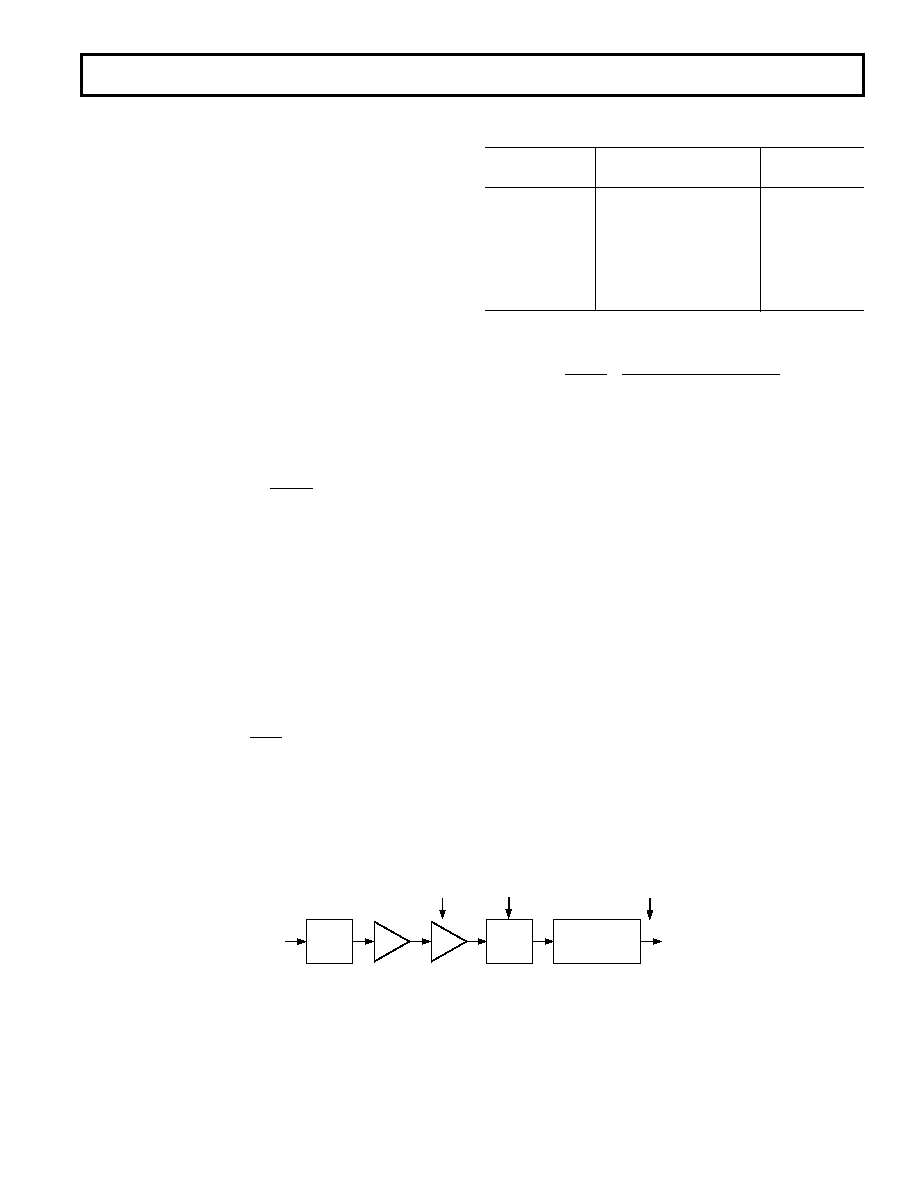
temperature change. A block diagram of the ADC input
channel with chop disabled is shown in Figure 10. The
signal chain includes a mux, buffer, PGA, sigma-delta modu-
lator, and digital filter. The modulator bit stream is applied to
a Sinc
3 filter. The programming of the Sinc3 decimation
factor is restricted to an 8-bit register SF, the actual decima-
tion factor is the register value times 8. The decimated output
rate from the Sinc
3 filter (and the ADC conversion rate) will there-
fore be:
f
SF
ADC
MOD
=
×
8
where
fADC is the ADC conversion rate,
SF is the decimal equivalent of the word loaded to the filter
register, valid range is from 3 to 255,
fMOD is the modulator sampling rate of 32.768 kHz.
The settling time to a step input is governed by the digital filter.
A synchronized step change will require a settling time of three
times the programmed update rate, a channel change can be
treated as a synchronized step change. An unsynchronized step
change will require four outputs to reflect the new analog input
at its output.
t
f
t
SETTLE
ADC
== ×
3
The allowable range for SF is 3 to 255 with a default of 69
(45H). The corresponding conversion rates, conversion times,
and settling times are shown in Table VI. Note that the conver-
sion time increases by 0.245 ms for each increment in SF.
Table VI. ADC Conversion and Settling Times for Various
SF Words with
CHOP = 1
SF
Data Update Rate
Settling Time
Word
fADC (Hz)
tSETTLE (ms)
03
1365.33
2.20
68
60.2
49.8
69 (Default)
59.36
50.54
75
54.6
54.93
82
49.95
60
151
27.13
110.6
255
16.06
186.76
The frequency response of the digital filter H (f) is as follows:
1
8
3
SF
f f
ff
MOD
×
×× ×
×
sin(
/
)
sin(
/
)
π
where
fMOD = 32,768 Hz,
SF = value programmed into SF SFR.
The following shows plots of the filter frequency response using
different SF words for output data rates of 16 Hz to 1.36 kHz.
There are sinc
3 notches at integer multiples of the update rate.
The 3 dB frequency for all values of SF obeys the following
equation:
f (3 dB) = 0.262
× fADC
The following plots show frequency response of the AD7708/
AD7718 digital filter for various filter words. The AD7708/
AD7718 are targeted at multiplexed applications. One of the
key requirements in these applications is to optimize the SF
word to obtain the maximum filter rejection at 50 Hz and 60 Hz
while minimizing the channel throughput rate. Figure 12 shows
the AD7708/AD7718 optimized throughput while maximizing
50 Hz and 60 Hz rejection. This is achieved with an SF word of
75. In Figure 13, by using a higher SF word of 151, 50 Hz and
60 Hz rejection can be maximized at 60 dB with a channel
throughput rate of 110 ms. An SF word of 255 gives maximum
rejection at both 50 Hz and 60 Hz but the channel throughput
rate is restricted to 186 ms as shown in Figure 14.
SINC3 FILTER
MUX
BUF
PGA
-
MOD0
ANALOG
INPUT
DIGITAL
OUTPUT
f
IN
f
MOD
f
ADC
Figure 10. ADC Channel Block Diagram with CHOP Disabled
相关PDF资料 |
PDF描述 |
|---|---|
| RPP20-4812D/N | CONV DC/DC 20W 36-75VIN +/-12V |
| EBA14DTKT-S288 | CONN EDGECARD 28POS .125 EXTEND |
| RPP20-4805S/N | CONV DC/DC 20W 36-75VIN 05VOUT |
| ECM12DRMT | CONN EDGECARD 24POS .156 WW |
| DEMO51AC256KIT | KIT DEMO DEMOAC DC9S08A |
相关代理商/技术参数 |
参数描述 |
|---|---|
| EVAL-AD7709EB | 制造商:Analog Devices 功能描述:EVAL KIT FOR 16BIT- ADC W/ SWITABLE CURRENT SOURCES - Bulk |
| EVAL-AD7710EB | 制造商:AD 制造商全称:Analog Devices 功能描述:Signal Conditioning ADC |
| EVAL-AD7711EB | 制造商:AD 制造商全称:Analog Devices 功能描述:LC2MOS Signal Conditioning ADC with RTD Excitation Currents |
| EVAL-AD7712EB | 制造商:AD 制造商全称:Analog Devices 功能描述:LC2MOS Signal Conditioning ADC |
| EVAL-AD7713EB | 制造商:AD 制造商全称:Analog Devices 功能描述:LC2MOS Loop-Powered Signal Conditioning ADC |
发布紧急采购,3分钟左右您将得到回复。