- 您现在的位置:买卖IC网 > PDF目录17060 > EVAL-AD7766-2EDZ (Analog Devices Inc)BOARD EVAL AD7766-2 32KSPS 114DB PDF资料下载
参数资料
| 型号: | EVAL-AD7766-2EDZ |
| 厂商: | Analog Devices Inc |
| 文件页数: | 16/25页 |
| 文件大小: | 0K |
| 描述: | BOARD EVAL AD7766-2 32KSPS 114DB |
| 标准包装: | 1 |
| ADC 的数量: | 1 |
| 位数: | 24 |
| 采样率(每秒): | 32k |
| 数据接口: | 串行 |
| 输入范围: | ±VREF |
| 在以下条件下的电源(标准): | 8.5mW @ 32kSPS |
| 工作温度: | -40°C ~ 105°C |
| 已用 IC / 零件: | AD7766-2 |
| 已供物品: | 板,CD |
| 相关产品: | AD7766BRUZ-2-ND - IC ADC 24BIT 32KSPS SAR 16TSSOP AD7766BRUZ-1-ND - IC ADC 24BIT 64KSPS SAR 16TSSOP AD7766BRUZ-ND - IC ADC 24BIT 128KSPS SAR 16TSSOP AD7766BRUZ-RL7-ND - IC ADC 24BIT 128KSPS SAR 16TSSOP AD7766BRUZ-2-RL7-ND - IC ADC 24BIT 32KSPS SAR 16TSSOP AD7766BRUZ-1-RL7-ND - IC ADC 24BIT 64KSPS SAR 16TSSOP |
AD7766
Rev. C | Page 22 of 24
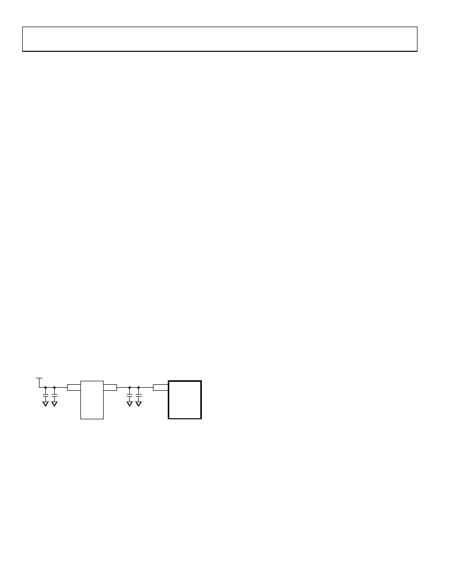
VREF+ INPUT SIGNAL
The AD7766/AD7766-1/AD7766-2 VREF + pin is supplied with a
voltage in the range of 2.4 V to 2 × AVDD (nominally 5 V). It is
recommended that the VREF+ input be generated by a low noise
voltage reference. Examples of such references are the ADR445,
Typical reference supply circuits are shown in Figure 46.
The reference voltage input pin (VREF+) also acts as a power
supply to the AD7766/AD7766-1/AD7766-2 devices. For a 5 V
VREF+ input, a full-scale input of 5 V on both VIN+ and VIN can
be applied while voltage supplies to pins AVDD remain at 2.5 V.
This configuration reduces the number of different supplies
required.
The output of the low noise voltage reference does not require a
buffer; however, decoupling the output of the low noise reference is
important. Place a 0.1 μF capacitor at the output of the voltage
and follow the decoupling advice provided for the reference
device chosen.
As mentioned, the nominal supply to the VREF+ pin is 5 V to
achieve the full dynamic range available. When a 2.5 V VREF+
input is used (that is, in low power applications), the signal-to-
noise ratio and dynamic range figures (generated using a 5 V
6 dB, a direct result of halving the available input range.
The AD7766/AD7766-1/AD7766-2 devices require a 100 μF
capacitor to ground, which acts as a decoupling capacitor and as
a reservoir of charge for the VREF+ pin. Place this capacitor as
close to the AD7766/AD7766-1/AD7766-2 devices as possible.
Reducing the value of this capacitor (C40 in Figure 46) to 10 μF
typically degrades noise performance by 1 dB. C40 can be an
electrolytic or tantalum capacitor.
06
44
9-
2
29
C39
0.1F
C40
100F
C34
10F
C35
0.1F
AD7766/
AD7766-1/
AD7766-2
ADR4xx
VOUT
V
REFERENCE
SUPPLY
V+
REF+
VIN
Figure 46. AD7766/AD7766-1/AD7766-2 Reference Input Configuration
MULTIPLEXING ANALOG INPUT CHANNELS
The AD7766/AD7766-1/AD7766-2 can be used with a multi-
plexer configuration. As per any converter that uses a digital
filtering block, the maximum switching rate or the output data
rate per channel is a function of the digital filter settling time.
A user multiplexing the analog inputs to a converter that
employs a digital filter must wait the full digital filter settling
time before a valid conversion result can be achieved; after this
settling time, the channel can be switched. Then, the full
settling time must again be observed before a valid conversion
result is available and the input is switched once more.
The AD7766 filter settling time equals 74 divided by the output
data rate in use. The maximum switching frequency in a multi-
plexed application is, therefore, 1/(74/ODR), where the output
data rate (ODR) is a function of the applied MCLK frequency
and the decimation rate employed by the device in question. For
example, applying a 1.024 MHz MCLK frequency to the AD7766
results in a maximum output data rate of 128 kHz, which in
turn allows a 1.729 kHz multiplexer switching rate.
The AD7766-1 and the AD7766-2 employ digital filters with
longer settling time to achieve greater precision; thus, the
maximum switching frequency for these devices is 864 Hz and
432 Hz, respectively.
相关PDF资料 |
PDF描述 |
|---|---|
| SLPX153M035E7P3 | CAP ALUM 15000UF 35V 20% SNAP |
| 0210490303 | CABLE JUMPER 1.25MM .076M 24POS |
| MIC2015-0.8YM6 TR | IC DISTRIBUTION SW 0.8A SOT23-6 |
| EVAL-AD7767-2EDZ | BOARD EVALUATION FOR AD7767 |
| VE-B34-EY | CONVERTER MOD DC/DC 48V 50W |
相关代理商/技术参数 |
参数描述 |
|---|---|
| EVAL-AD7766EDZ | 功能描述:BOARD EVAL AD7766 128KSPS 108DB RoHS:是 类别:编程器,开发系统 >> 评估板 - 模数转换器 (ADC) 系列:- 产品培训模块:Obsolescence Mitigation Program 标准包装:1 系列:- ADC 的数量:1 位数:12 采样率(每秒):94.4k 数据接口:USB 输入范围:±VREF/2 在以下条件下的电源(标准):- 工作温度:-40°C ~ 85°C 已用 IC / 零件:MAX11645 已供物品:板,软件 |
| EVAL-AD7767-1EDZ | 功能描述:BOARD EVAL AD7767-1 64KSPS 111DB RoHS:是 类别:编程器,开发系统 >> 评估板 - 模数转换器 (ADC) 系列:- 产品培训模块:Obsolescence Mitigation Program 标准包装:1 系列:- ADC 的数量:1 位数:12 采样率(每秒):94.4k 数据接口:USB 输入范围:±VREF/2 在以下条件下的电源(标准):- 工作温度:-40°C ~ 85°C 已用 IC / 零件:MAX11645 已供物品:板,软件 |
| EVAL-AD7767-2EDZ | 功能描述:BOARD EVALUATION FOR AD7767 RoHS:是 类别:编程器,开发系统 >> 评估板 - 模数转换器 (ADC) 系列:- 产品培训模块:Obsolescence Mitigation Program 标准包装:1 系列:- ADC 的数量:1 位数:12 采样率(每秒):94.4k 数据接口:USB 输入范围:±VREF/2 在以下条件下的电源(标准):- 工作温度:-40°C ~ 85°C 已用 IC / 零件:MAX11645 已供物品:板,软件 |
| EVAL-AD7767EDZ | 功能描述:BOARD EVAL AD7767 128KSPS 108DB RoHS:是 类别:编程器,开发系统 >> 评估板 - 模数转换器 (ADC) 系列:- 产品培训模块:Obsolescence Mitigation Program 标准包装:1 系列:- ADC 的数量:1 位数:12 采样率(每秒):94.4k 数据接口:USB 输入范围:±VREF/2 在以下条件下的电源(标准):- 工作温度:-40°C ~ 85°C 已用 IC / 零件:MAX11645 已供物品:板,软件 |
| EVAL-AD7780EBZ | 功能描述:BOARD EVAL FOR AD7780 RoHS:是 类别:编程器,开发系统 >> 评估板 - 模数转换器 (ADC) 系列:- 产品培训模块:Obsolescence Mitigation Program 标准包装:1 系列:- ADC 的数量:1 位数:12 采样率(每秒):94.4k 数据接口:USB 输入范围:±VREF/2 在以下条件下的电源(标准):- 工作温度:-40°C ~ 85°C 已用 IC / 零件:MAX11645 已供物品:板,软件 |
发布紧急采购,3分钟左右您将得到回复。