- 您现在的位置:买卖IC网 > PDF目录17049 > EVAL-AD7986EBZ (Analog Devices Inc)BOARD EVAL FOR AD7986 PDF资料下载
参数资料
| 型号: | EVAL-AD7986EBZ |
| 厂商: | Analog Devices Inc |
| 文件页数: | 7/28页 |
| 文件大小: | 0K |
| 描述: | BOARD EVAL FOR AD7986 |
| 产品培训模块: | Motor Control |
| 标准包装: | 1 |
| 系列: | PulSAR® |
| ADC 的数量: | 1 |
| 位数: | 18 |
| 采样率(每秒): | 2M |
| 数据接口: | 串行 |
| 输入范围: | ±VREF |
| 在以下条件下的电源(标准): | 29mW @ 2MSPS |
| 工作温度: | -40°C ~ 85°C |
| 已用 IC / 零件: | AD7986 |
| 已供物品: | 板 |
第1页第2页第3页第4页第5页第6页当前第7页第8页第9页第10页第11页第12页第13页第14页第15页第16页第17页第18页第19页第20页第21页第22页第23页第24页第25页第26页第27页第28页
AD7986
Rev. B | Page 15 of 28
ANALOG INPUTS
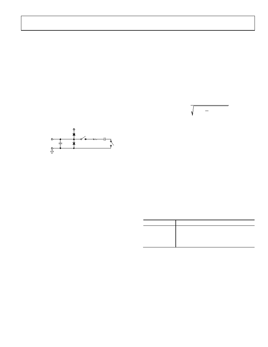
Figure 24 shows an equivalent circuit of the input structure of
the AD7986.
The two diodes, D1 and D2, provide ESD protection for the
analog inputs, IN+ and IN. Care must be taken to ensure that
the analog input signal does not exceed the reference input
voltage (REF) by more than 0.3 V. If the analog input signal
exceeds this level, the diodes become forward-biased and start
conducting current. These diodes can handle a forward-biased
current of 130 mA maximum. However, if the supplies of the
input buffer (for example, the V+ and V supplies of the buffer
amplifier in Figure 23) are different from those of REF, the
analog input signal may eventually exceed the supply rails by
more than 0.3 V. In such a case (for example, an input buffer
with a short circuit), the current limitation can be used to
protect the part.
CPIN
REF
RIN
CIN
D1
D2
IN+ OR IN–
GND
07956-
014
Figure 24. Equivalent Analog Input Circuit
The analog input structure allows the sampling of the true
differential signal between IN+ and IN. By using these
differential inputs, signals common to both inputs are rejected.
During the acquisition phase, the impedance of the analog
inputs (IN+ or IN) can be modeled as a parallel combination
of Capacitor CPIN and the network formed by the series connection
of RIN and CIN. CPIN is primarily the pin capacitance. RIN is typically
400 and is a lumped component composed of serial resistors
and the on resistance of the switches. CIN is typically 30 pF and
is mainly the ADC sampling capacitor.
During the sampling phase, where the switches are closed, the
input impedance is limited to CPIN. RIN and CIN make a one-pole,
low-pass filter that reduces undesirable aliasing effects and
limits noise.
When the source impedance of the driving circuit is low, the
AD7986 can be driven directly. Large source impedances
significantly affect the ac performance, especially THD. The
dc performances are less sensitive to the input impedance. The
maximum source impedance depends on the amount of THD
that can be tolerated. The THD degrades as a function of the
source impedance and the maximum input frequency.
DRIVER AMPLIFIER CHOICE
Although the AD7986 is easy to drive, the driver amplifier must
meet the following requirements:
The noise generated by the driver amplifier must be kept as
low as possible to preserve the SNR and transition noise
performance of the AD7986. The noise from the driver is
filtered by the AD7986 analog input circuit’s one-pole, low-
pass filter, made by RIN and CIN or by the external filter, if
one is used. Because the typical noise of the AD7986 is
62.5 V rms, the SNR degradation due to the amplifier is
+
=
2
)
(
2
π
.4
4
3
62.5
log
20
N
3dB
LOSS
Ne
f
SNR
where:
f–3dB is the input bandwidth, in megahertz, of the AD7986
(20 MHz) or the cutoff frequency of the input filter, if
one is used.
N is the noise gain of the amplifier (for example, 1 in buffer
configuration).
eN is the equivalent input noise voltage of the op amp, in
nV/√Hz.
For ac applications, the driver should have a THD perfor-
mance commensurate with the AD7986.
For multichannel multiplexed applications, the driver
amplifier and the AD7986 analog input circuit must settle
for a full-scale step onto the capacitor array at an 18-bit level
(0.0004%, 4 ppm). In the data sheet of the driver amplifier,
settling at 0.1% to 0.01% is more commonly specified. This
may differ significantly from the settling time at an 18-bit
level and should be verified prior to driver selection.
Table 8. Recommended Driver Amplifiers
Amplifier
Typical Application
Very low noise and high frequency
Low noise and high frequency
Ultralow noise and high frequency
Low power and high frequency
相关PDF资料 |
PDF描述 |
|---|---|
| HKQ0603S1N3C-T | INDUCTOR HI FREQ 1.3NH 0201 |
| MPC8313E-RDB | BOARD PROCESSOR |
| STD01W-J | WIRE & CABLE MARKERS |
| STD09W-C | WIRE & CABLE MARKERS |
| STD09W-T | WIRE & CABLE MARKERS |
相关代理商/技术参数 |
参数描述 |
|---|---|
| EVAL-AD7988-5SDZ | 功能描述:BAORD EVAL FOR AD7988-5 RoHS:是 类别:编程器,开发系统 >> 评估板 - 模数转换器 (ADC) 系列:PulSAR® 产品培训模块:Obsolescence Mitigation Program 标准包装:1 系列:- ADC 的数量:1 位数:12 采样率(每秒):94.4k 数据接口:USB 输入范围:±VREF/2 在以下条件下的电源(标准):- 工作温度:-40°C ~ 85°C 已用 IC / 零件:MAX11645 已供物品:板,软件 |
| EVAL-AD7991EBZ | 功能描述:BOARD EVAL FOR AD7991 RoHS:是 类别:编程器,开发系统 >> 评估板 - 模数转换器 (ADC) 系列:- 产品培训模块:Obsolescence Mitigation Program 标准包装:1 系列:- ADC 的数量:1 位数:12 采样率(每秒):94.4k 数据接口:USB 输入范围:±VREF/2 在以下条件下的电源(标准):- 工作温度:-40°C ~ 85°C 已用 IC / 零件:MAX11645 已供物品:板,软件 |
| EVAL-AD7991EBZ | 制造商:Analog Devices 功能描述:AD7991, ADC, I2C, EVALUATION BOARD |
| EVAL-AD7992CB | 制造商:AD 制造商全称:Analog Devices 功能描述:2-Channel, 12-Bit ADC with I2C-Compatible |
| EVAL-AD7992EBZ | 功能描述:BOARD EVALUATION FOR AD7992 RoHS:是 类别:编程器,开发系统 >> 评估板 - 模数转换器 (ADC) 系列:- 产品培训模块:Obsolescence Mitigation Program 标准包装:1 系列:- ADC 的数量:1 位数:12 采样率(每秒):94.4k 数据接口:USB 输入范围:±VREF/2 在以下条件下的电源(标准):- 工作温度:-40°C ~ 85°C 已用 IC / 零件:MAX11645 已供物品:板,软件 |
发布紧急采购,3分钟左右您将得到回复。