- 您现在的位置:买卖IC网 > PDF目录17048 > EVAL-AD7992EBZ (Analog Devices Inc)BOARD EVALUATION FOR AD7992 PDF资料下载
参数资料
| 型号: | EVAL-AD7992EBZ |
| 厂商: | Analog Devices Inc |
| 文件页数: | 13/29页 |
| 文件大小: | 0K |
| 描述: | BOARD EVALUATION FOR AD7992 |
| 标准包装: | 1 |
| ADC 的数量: | 1 |
| 位数: | 12 |
| 采样率(每秒): | 188k |
| 数据接口: | I²C,串行 |
| 输入范围: | 0 ~ VREF |
| 在以下条件下的电源(标准): | 7.7mW @ 188kSPS,5.5 V |
| 工作温度: | -40°C ~ 125°C |
| 已用 IC / 零件: | AD7992 |
| 已供物品: | 板,线缆 |
第1页第2页第3页第4页第5页第6页第7页第8页第9页第10页第11页第12页当前第13页第14页第15页第16页第17页第18页第19页第20页第21页第22页第23页第24页第25页第26页第27页第28页第29页
AD7992
Rev. 0 | Page 19 of 28
Using the Limit Registers to Store Min/Max Conversion
Results
If full scale—that is, all 1s—is written to the hysteresis register
for a particular channel, the DATAHIGH and DATALOW registers
for that channel no longer act as limit registers as previously
described, but instead act as storage registers for the maximum
and minimum conversion results returned from conversions on
a channel over any given period of time. This function is useful
in applications where the widest span of actual conversion
results is required rather than using the ALERT to signal that an
intervention is necessary—for example, when monitoring
temperature extremes during refrigerated goods transportation.
Note that on power-up, the contents of the DATAHIGH register
for each channel are full scale, while the contents of the
DATALOW registers are zero scale by default. Therefore, min-
imum and maximum conversion values being stored in this
way are lost if power is removed or cycled.
ALERT STATUS REGISTER
The alert status register is an 8-bit read/write register that
provides information on an alert event. If a conversion results in
activating the ALERT pin or Alert_Flag bit in the conversion
result register (see the Limit Registers section) the alert status
register may be read to gain further information. It contains
two status bits per channel, one corresponding to each of the
DATAHIGH and DATALOW limits. The bit with a status of 1 shows
where the violation occurred—that is, on which channel—and
whether the violation occurred on the upper or lower limit.
If a second alert event occurs on the other channel between
receiving the first alert and interrogating the alert status
register, the corresponding bit for that alert event is also set.
The entire contents of the alert status register can be cleared by
writing 1,1 to Bits D2 and D1 in the configuration register, as
shown in Table 11. This can also be achieved by writing all 1s to
the alert status register itself. Thus, if the alert status register is
addressed for a write operation, which is all 1s, the contents of
the alert status register are cleared or reset to all 0s.
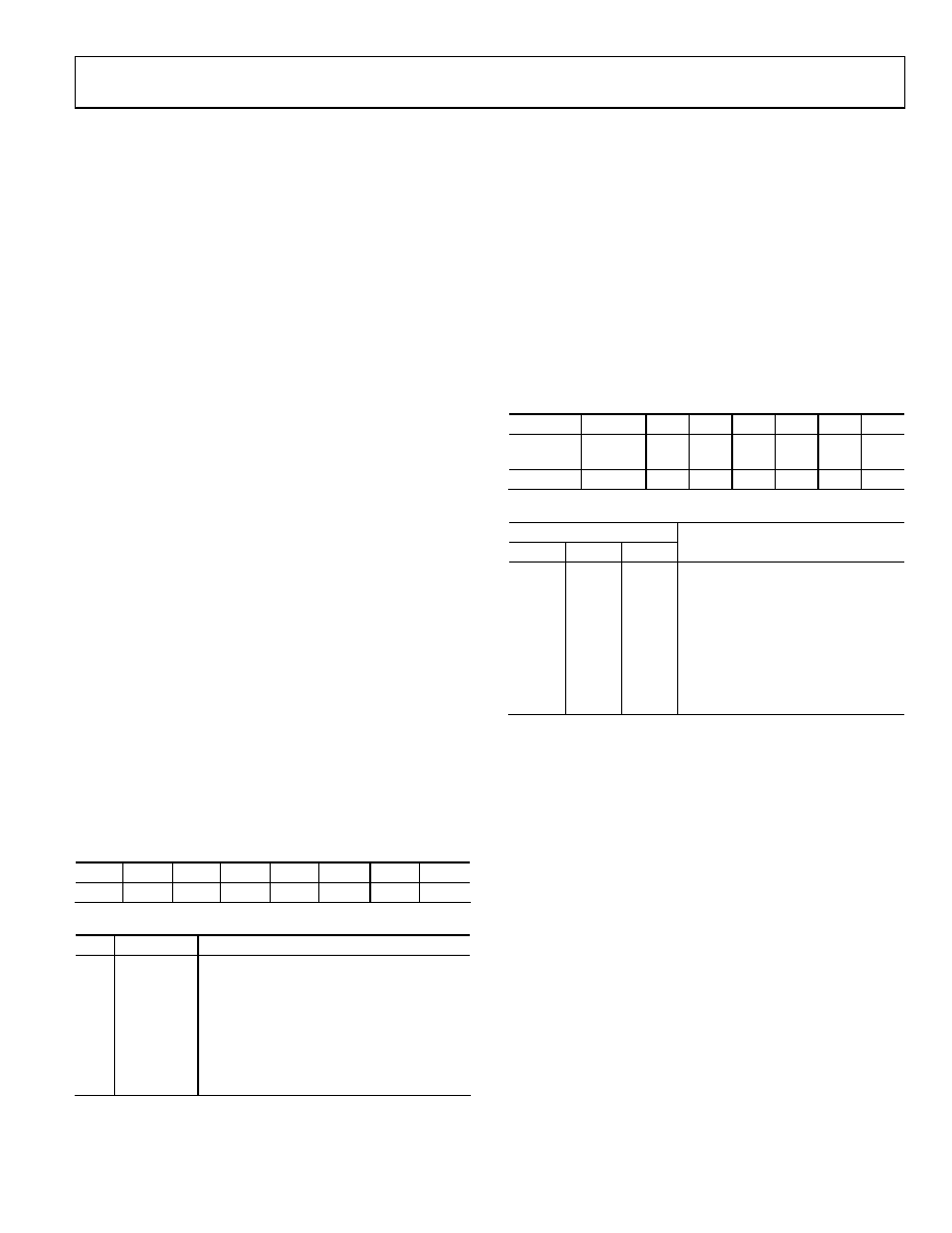
Table 20. Alert Status Register
D7
D6
D5
D4
D3
D2
D1
D0
0
CH2HI
CH2LO
CH1HI
CH1LO
Table 21. Alert Status Register Bit Function Descriptions
Bit
Mnemonic
Comment
D0
CH1LO
Violation of DATALOW limit on Channel 1 if
bit is set to 1, no violation if bit is set to 0.
D1
CH1HI
Violation of DATAHIGH limit on Channel 1 if
bit is set to 1, no violation if bit is set to 0.
D2
CH2LO
Violation of DATALOW limit on Channel 2 if
bit is set to 1, no violation if bit is set to 0.
D3
CH2HI
Violation of DATAHIGH limit on Channel 2 if
bit is set to 1, no violation if bit is set to 0.
CYCLE TIMER REGISTER
The cycle timer register is an 8-bit read/write register that stores
the conversion interval value for the automatic cycle mode of
the AD7992 (see the Modes of Operation section). The 5 MSBs
of the cycle timer register are unused and should contain 0s at
all times (see the Sample Delay and Bit Trial Delay section). On
power-up, the cycle timer register contains all 0s, thus disabling
automatic cycle operation of the AD7992. To enable automatic
cycle mode, the user must write to the cycle timer register,
selecting the required conversion interval. Table 22 shows the
structure of the cycle timer register, while Table 23 shows how
the bits in this register are decoded to provide various
automatic sampling intervals.
Table 22. Cycle Timer Register and Defaults at Power-Up
D7
D6
D5
D4
D3
D2
D1
D0
Sample
Delay
Bit Trial
Delay
0
Cyc
Bit 2
Cyc
Bit 1
Cyc
Bit 0
0
Table 23. Cycle Timer Intervals
CYC Reg Value
Conversion Interval
D2
D1
D0
(TCONVERT =conversion time of ADC)
0
Mode not selected
0
1
TCONVERT × 32
0
1
0
TCONVERT × 64
0
1
TCONVERT × 128
1
0
TCONVERT × 256
1
0
1
TCONVERT × 512
1
0
TCONVERT × 1024
1
TCONVERT × 2048
SAMPLE DELAY AND BIT TRIAL DELAY
It is recommended that no I2C bus activity occurs when a
conversion is taking place. However, this may not be possible,
for example, when operating in Mode 2 or the automatic cycle
mode. In order to maintain the performance of the ADC in
such cases, Bits D7 and D6 in the cycle timer register are used
to delay critical sample intervals and bit trials from occurring
while there is activity on the I2C bus. This may have the effect of
increasing the conversion time. When Bits D7 and D6 are both
0, the bit trial and sample interval delaying mechanism are
implemented. The default setting of D7 and D6 is 0. If bit trial
delays extend longer than 1 s, the conversion terminates.
When D7 is 0, the sampling instant delay is implemented.
When D6 is 0, the bit trial delay is implemented. To turn off
both the sample delay and bit trial delay, set D7 and D6 to 1.
相关PDF资料 |
PDF描述 |
|---|---|
| EBC10DRAH-S734 | CONN EDGECARD 20POS .100 R/A PCB |
| 0210490902 | CABLE JUMPER 1.25MM .076M 21POS |
| 0210390992 | CABLE JUMPER 1MM .102M 29POS |
| HKQ0603S2N3C-T | INDUCTOR HI FREQ 2.3NH 0201 |
| 0982660877 | CBL 19PS 0.5MM JMPR TYPE A 1.18" |
相关代理商/技术参数 |
参数描述 |
|---|---|
| EVAL-AD7993CB | 制造商:Analog Devices 功能描述:EVALUATION CONTROL BOARD. - Bulk |
| EVAL-AD7993CBZ | 制造商:Analog Devices 功能描述:EVALUATION CONTROL BOARD. - Bulk |
| EVAL-AD7993EBZ | 功能描述:BOARD EVAL FOR AD7993 RoHS:是 类别:编程器,开发系统 >> 评估板 - 模数转换器 (ADC) 系列:- 产品培训模块:Obsolescence Mitigation Program 标准包装:1 系列:- ADC 的数量:1 位数:12 采样率(每秒):94.4k 数据接口:USB 输入范围:±VREF/2 在以下条件下的电源(标准):- 工作温度:-40°C ~ 85°C 已用 IC / 零件:MAX11645 已供物品:板,软件 |
| EVAL-AD7994CB | 制造商:Analog Devices 功能描述:EVALUATION CONTROL BOARD. - Bulk |
| EVAL-AD7994CBZ | 制造商:Analog Devices 功能描述:EVALUATION CONTROL BOARD. - Bulk |
发布紧急采购,3分钟左右您将得到回复。