- 您现在的位置:买卖IC网 > PDF目录17048 > EVAL-AD7992EBZ (Analog Devices Inc)BOARD EVALUATION FOR AD7992 PDF资料下载
参数资料
| 型号: | EVAL-AD7992EBZ |
| 厂商: | Analog Devices Inc |
| 文件页数: | 29/29页 |
| 文件大小: | 0K |
| 描述: | BOARD EVALUATION FOR AD7992 |
| 标准包装: | 1 |
| ADC 的数量: | 1 |
| 位数: | 12 |
| 采样率(每秒): | 188k |
| 数据接口: | I²C,串行 |
| 输入范围: | 0 ~ VREF |
| 在以下条件下的电源(标准): | 7.7mW @ 188kSPS,5.5 V |
| 工作温度: | -40°C ~ 125°C |
| 已用 IC / 零件: | AD7992 |
| 已供物品: | 板,线缆 |
第1页第2页第3页第4页第5页第6页第7页第8页第9页第10页第11页第12页第13页第14页第15页第16页第17页第18页第19页第20页第21页第22页第23页第24页第25页第26页第27页第28页当前第29页
AD7992
Rev. 0 | Page 8 of 28
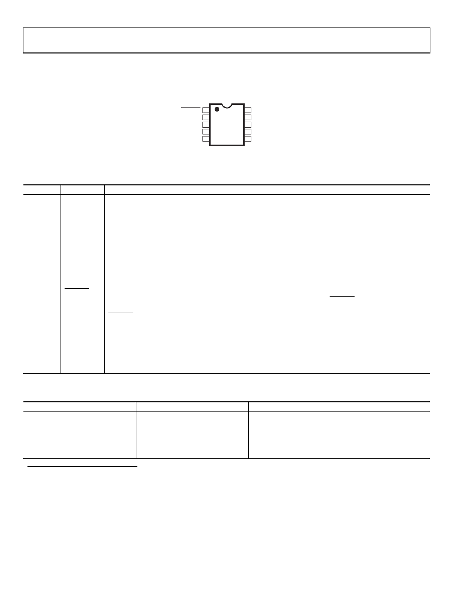
PIN CONFIGURATION AND PIN FUNCTION DESCRIPTIONS
AD7992
TOP VIEW
1
2
3
4
7
8
9
10
SDA
SCL
VDD
AGND
5
(Not to Scale)
ALERT
6
AS
VIN1
VIN2/REFIN
03263-0-002
CONVST
Figure 3. AD7992 Pin Configuration
Table 5. Pin Function Descriptions
Pin No.
Mnemonic
Function
2, 7
AGND
Analog Ground. Ground reference point for all circuitry on the AD7992. All analog input signals should be
referred to this GND voltage.
3
VDD
Power Supply Input. The VDD range for the AD7992 is from 2.7 V to 5.5 V.
4
VIN2/REFIN
Analog Input 2/Voltage Reference Input. In single-channel mode, this pin becomes the reference voltage input;
an external reference should be applied at this pin. The external reference input range is 1.2 V to VDD. A 0.1 F
and 1F capacitor should be tied between this pin and AGND. If Bit D6 is set to 1 in the configuration register,
the AD7992 operates in single-channel mode. In dual-channel mode, D6 in the configuration register is 0; in
this case, this pin provides the second analog input channel. The reference voltage for the AD7992 is taken
from the power supply voltage in dual-channel mode. See the Configuration Register section and Table 10.
5
VIN1
Analog Input 1. Single-ended analog input channel. The input range is 0 V to REFIN.
6
AS
Logic Input. Address select input that selects one of three I2C addresses for the AD7992, as shown in Table 6.
1
CONVST
Logic Input Signal. Convert start signal. This is an edge-triggered logic input. The rising edge of this signal
powers up the part. The power up time for the part is 1 s. The falling edge of CONVST places the track-and-
hold into hold mode and initiates a conversion. A power-up time of at least 1 s must be allowed for the
CONVST high pulse; otherwise, the conversion result is invalid (see the Modes of Operation section).
8
ALERT/BUSY
Digital Output. Selectable as an ALERT or BUSY output function. When configured as an ALERT, this pin acts as
an out-of-range indicator and, if enabled, becomes active when the conversion result violates the DATAHIGH or
DATALOW register values. See the Limit Registers section. When configured as a BUSY output, this pin becomes
active when a conversion is in progress. Open-drain output. An external pull-up resistor is required.
9
SDA
Digital I/O. Serial bus bidirectional data. Open-drain output. An external pull-up resistor is required.
10
SCL
Digital Input. Serial bus clock. Open-drain output. An external pull-up resistor is required.
Table 6. I2C Address Selection
Part Number
AS Pin
I2C Address
AD7992-0
GND
010 0001
AD7992-0
VDD
010 0010
AD7992-1
GND
010 0011
AD7992-1
VDD
010 0100
AD7992-x1
Float
010 0000
1 If the AS pin is left floating on any of the AD7992 parts, the device address is 010 0000. This gives each AD7992 device three different address options.
相关PDF资料 |
PDF描述 |
|---|---|
| EBC10DRAH-S734 | CONN EDGECARD 20POS .100 R/A PCB |
| 0210490902 | CABLE JUMPER 1.25MM .076M 21POS |
| 0210390992 | CABLE JUMPER 1MM .102M 29POS |
| HKQ0603S2N3C-T | INDUCTOR HI FREQ 2.3NH 0201 |
| 0982660877 | CBL 19PS 0.5MM JMPR TYPE A 1.18" |
相关代理商/技术参数 |
参数描述 |
|---|---|
| EVAL-AD7993CB | 制造商:Analog Devices 功能描述:EVALUATION CONTROL BOARD. - Bulk |
| EVAL-AD7993CBZ | 制造商:Analog Devices 功能描述:EVALUATION CONTROL BOARD. - Bulk |
| EVAL-AD7993EBZ | 功能描述:BOARD EVAL FOR AD7993 RoHS:是 类别:编程器,开发系统 >> 评估板 - 模数转换器 (ADC) 系列:- 产品培训模块:Obsolescence Mitigation Program 标准包装:1 系列:- ADC 的数量:1 位数:12 采样率(每秒):94.4k 数据接口:USB 输入范围:±VREF/2 在以下条件下的电源(标准):- 工作温度:-40°C ~ 85°C 已用 IC / 零件:MAX11645 已供物品:板,软件 |
| EVAL-AD7994CB | 制造商:Analog Devices 功能描述:EVALUATION CONTROL BOARD. - Bulk |
| EVAL-AD7994CBZ | 制造商:Analog Devices 功能描述:EVALUATION CONTROL BOARD. - Bulk |
发布紧急采购,3分钟左右您将得到回复。