- 您现在的位置:买卖IC网 > PDF目录17048 > EVAL-AD7992EBZ (Analog Devices Inc)BOARD EVALUATION FOR AD7992 PDF资料下载
参数资料
| 型号: | EVAL-AD7992EBZ |
| 厂商: | Analog Devices Inc |
| 文件页数: | 6/29页 |
| 文件大小: | 0K |
| 描述: | BOARD EVALUATION FOR AD7992 |
| 标准包装: | 1 |
| ADC 的数量: | 1 |
| 位数: | 12 |
| 采样率(每秒): | 188k |
| 数据接口: | I²C,串行 |
| 输入范围: | 0 ~ VREF |
| 在以下条件下的电源(标准): | 7.7mW @ 188kSPS,5.5 V |
| 工作温度: | -40°C ~ 125°C |
| 已用 IC / 零件: | AD7992 |
| 已供物品: | 板,线缆 |
第1页第2页第3页第4页第5页当前第6页第7页第8页第9页第10页第11页第12页第13页第14页第15页第16页第17页第18页第19页第20页第21页第22页第23页第24页第25页第26页第27页第28页第29页
AD7992
Rev. 0 | Page 13 of 28
CIRCUIT INFORMATION
The AD7992 is a low power, 12-bit, single-supply, 2-channel
analog-to-digital converter (ADC). The part can be operated
from a 2.7 V to 5.5 V supply.
The AD7992 provides the user with a 2-channel multiplexer,
an on-chip track-and-hold, an ADC, an on-chip oscillator,
internal data registers, and an I2C-compatible serial interface,
all housed in a 10-lead MSOP package that offers the user
considerable space-saving advantages over alternative solutions.
The AD7992 requires an external reference in the range of 1.2 V
to VDD.
The AD7992 normally remains in a power-down state while not
converting. When supplies are first applied, the part comes up
in a power-down state. Power-up is initiated prior to a con-
version, and the device returns to power-down upon
completion of the conversion. Conversions can be initiated on
the AD7992 by pulsing the CONVST signal, using an automatic
cycle interval mode or a command mode where wake-up and a
conversion occur during a write address function (see the
Modes of Operation section). On completion of a conversion,
the AD7992 again enters power-down mode. This automatic
power-down feature allows power saving between conversions.
This means any read or write operations across the I2C interface
can occur while the device is in power-down.
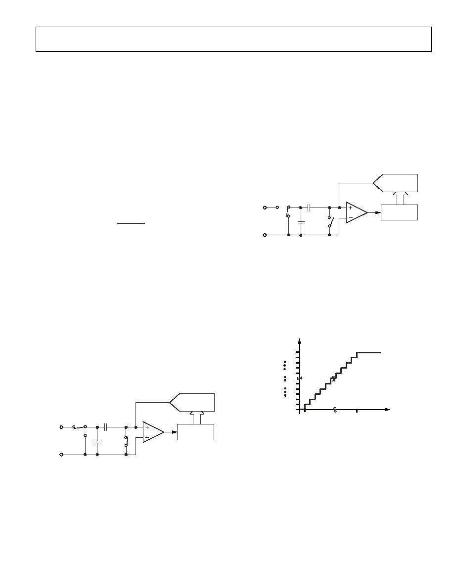
CONVERTER OPERATION
The AD7992 is a successive approximation, analog-to-digital
converter based around a capacitive DAC. Figure 17 and
Figure 18 show simplified schematics of the ADC during its
acquisition and conversion phases, respectively. Figure 17 shows
the ADC during its acquisition phase. SW2 is closed and SW1 is
in position A, the comparator is held in a balanced condition,
and the sampling capacitor acquires the signal on VIN.
CAPACITIVE
DAC
VIN
COMPARATOR
CONTROL
LOGIC
SW1
A
B
SW2
AGND
03473-0-018
Figure 17. ADC Acquisition Phase
When the ADC starts a conversion, as shown in Figure 18,
SW2 opens and SW1 moves to position B, causing the
comparator to become unbalanced. The input is disconnected
once the conversion begins. The control logic and the capacitive
DAC are used to add and subtract fixed amounts of charge from
the sampling capacitor to bring the comparator back into a
balanced condition. When the comparator is rebalanced, the
conversion is complete. The control logic generates the ADC
output code. Figure 19 shows the ADC transfer function.
VIN
COMPARATOR
CONTROL
LOGIC
SW1
A
B
SW2
AGND
CAPACITIVE
DAC
03473-0-019
Figure 18. ADC Conversion Phase
ADC Transfer Function
The output coding of the AD7992 is straight binary. The
designed code transitions occur at successive integer LSB values
(i.e., 1 LSB, 2 LSB, and so on). The LSB size for the AD7992 is
the AD7992.
000...000
ADC
CODE
ANALOG INPUT
0V TO REFIN
111...111
000...001
000...010
111...110
111...000
011...111
AGND + 1LSB
+REFIN – 1LSB
AD7992 1LSB = REFIN/4096
03263-0-003
Figure 19. AD7992 Transfer Characteristic
相关PDF资料 |
PDF描述 |
|---|---|
| EBC10DRAH-S734 | CONN EDGECARD 20POS .100 R/A PCB |
| 0210490902 | CABLE JUMPER 1.25MM .076M 21POS |
| 0210390992 | CABLE JUMPER 1MM .102M 29POS |
| HKQ0603S2N3C-T | INDUCTOR HI FREQ 2.3NH 0201 |
| 0982660877 | CBL 19PS 0.5MM JMPR TYPE A 1.18" |
相关代理商/技术参数 |
参数描述 |
|---|---|
| EVAL-AD7993CB | 制造商:Analog Devices 功能描述:EVALUATION CONTROL BOARD. - Bulk |
| EVAL-AD7993CBZ | 制造商:Analog Devices 功能描述:EVALUATION CONTROL BOARD. - Bulk |
| EVAL-AD7993EBZ | 功能描述:BOARD EVAL FOR AD7993 RoHS:是 类别:编程器,开发系统 >> 评估板 - 模数转换器 (ADC) 系列:- 产品培训模块:Obsolescence Mitigation Program 标准包装:1 系列:- ADC 的数量:1 位数:12 采样率(每秒):94.4k 数据接口:USB 输入范围:±VREF/2 在以下条件下的电源(标准):- 工作温度:-40°C ~ 85°C 已用 IC / 零件:MAX11645 已供物品:板,软件 |
| EVAL-AD7994CB | 制造商:Analog Devices 功能描述:EVALUATION CONTROL BOARD. - Bulk |
| EVAL-AD7994CBZ | 制造商:Analog Devices 功能描述:EVALUATION CONTROL BOARD. - Bulk |
发布紧急采购,3分钟左右您将得到回复。