- 您现在的位置:买卖IC网 > PDF目录16543 > EVAL-ADF4157EB1Z (Analog Devices Inc)BOARD EVALUATION FOR ADF4157 PDF资料下载
参数资料
| 型号: | EVAL-ADF4157EB1Z |
| 厂商: | Analog Devices Inc |
| 文件页数: | 11/24页 |
| 文件大小: | 0K |
| 描述: | BOARD EVALUATION FOR ADF4157 |
| 标准包装: | 1 |
| 主要目的: | 计时,频率合成器 |
| 嵌入式: | 否 |
| 已用 IC / 零件: | ADF4157 |
| 主要属性: | 单路分数-N PLL |
| 次要属性: | 6GHz |
| 已供物品: | 板 |
| 相关产品: | ADF4157BRUZ-ND - IC PLL FREQ SYNTH 6GHZ 16TSSOP ADF4157BRUZ-RL7-ND - IC PLL FREQ SYNTH 6GHZ 16TSSOP ADF4157BRUZ-RL-ND - IC PLL FREQ SYNTH 6GHZ 16TSSOP |
Data Sheet
ADF4157
Rev. D | Page 19 of 24
FASTLOCK TIMER AND REGISTER SEQUENCES
If the fastlock mode is used, a timer value needs to be loaded into
the PLL to determine the time spent in wide bandwidth mode.
When Bits DB[20:19] in Register 4 (R4) are set to 01 (switched
R fastlock enable), the timer value is loaded via the 12-bit clock
divider value. To use fastlock, the PLL must be written to in the
following sequence:
1. Use the initialization sequence (see the Initialization
Sequence section) only once after powering up the part.
2. Load Register 4 (R4) with Bits DB[20:19] set to 01 and the
chosen fastlock timer value (DB18 to DB7). Note that the
duration that the PLL remains in wide bandwidth is equal
to the fastlock timer/fPFD.
FASTLOCK: AN EXAMPLE
If a PLL has fPFD = 13 MHz and a required lock time of 50 s,
the PLL is set to wide bandwidth for 40 s.
If the time period set for the wide bandwidth is 40 s, then
Fastlock Timer Value = Time in Wide Bandwidth × fPFD
Fastlock Timer Value = 40 s × 13 MHz = 520
Therefore, 520 must be loaded into the clock divider value in
Register 4 (R4) in Step 2 of the sequence described in the
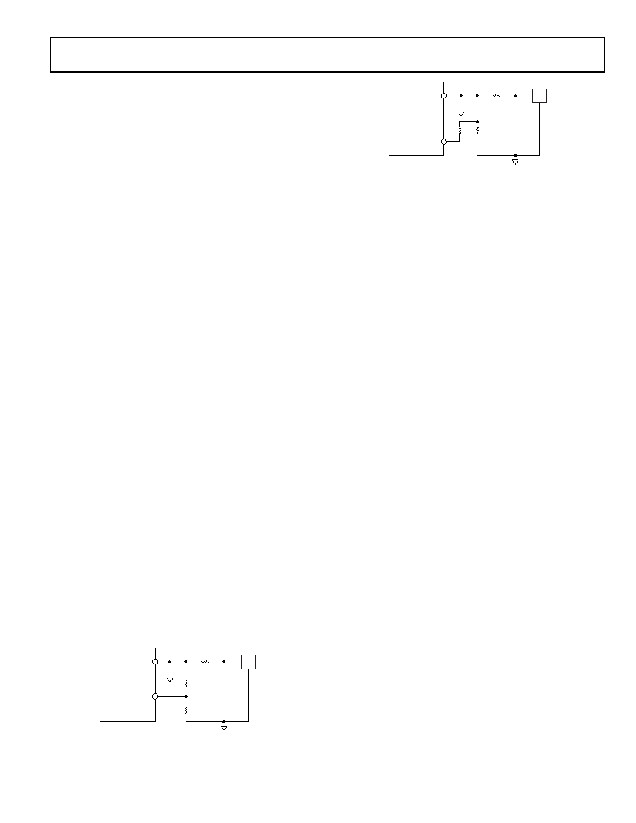
FASTLOCK: LOOP FILTER TOPOLOGY
To use fast-lock mode, an extra connection from the PLL to the
loop filter is needed. The damping resistor in the loop filter must
be reduced to of its value while in wide bandwidth mode. This is
required because the charge pump current is increased by 16
while in wide bandwidth mode, and stability must be ensured.
During fastlock, the MUXOUT pin (after setting MUXOUT to
fastlock switch by setting Bits DB[30:27] in Register 0 to 1100) is
shorted to ground (this is accomplished by settings Bits DB[20:19]
in Register 4 to 01—switched R fastlock enable). The following
two topologies can be used:
Divide the damping resistor (R1) into two values (R1 and
R1A) that have a ratio of 1:3 (see Figure 22).
Connect an extra resistor (R1A) directly from MUXOUT,
as shown in Figure 23. The extra resistor must be chosen
such that the parallel combination of an extra resistor and
the damping resistor (R1) is reduced to of the original
value of R1 (see Figure 23).
ADF4157
CP
MUXOUT
C1
C2
R2
R1
R1A
C3
VCO
05874-
022
Figure 22. Fast-Lock Loop Filter Topology—Topology 1
ADF4157
CP
MUXOUT
C1
C2
R2
R1
R1A
C3
VCO
05874-
023
Figure 23. Fastlock Loop Filter Topology—Topology 2
SPUR MECHANISMS
The fractional interpolator in the ADF4157 is a third-order Σ-Δ
modulator (SDM) with a 25-bit fixed modulus (MOD). The
SDM is clocked at the PFD reference rate (fPFD) that allows PLL
output frequencies to be synthesized at a channel step resolution of
fPFD/MOD. The various spur mechanisms possible with fractional-
N synthesizers, and how they affect the ADF4157, are discussed in
this section.
Fractional Spurs
In most fractional synthesizers, fractional spurs can appear at
the set channel spacing of the synthesizer. In the ADF4157,
these spurs do not appear. The high value of the fixed modulus
in the ADF4157 makes the Σ-Δ modulator quantization error
spectrum look like broadband noise, effectively spreading the
fractional spurs into noise.
Integer Boundary Spurs
Interactions between the RF VCO frequency and the PFD fre-
quency can lead to spurs known as integer boundary spurs. When
these frequencies are not integer related (which is the purpose
of the fractional-N synthesizer), spur sidebands appear on the
VCO output spectrum at an offset frequency that corresponds
to the beat note or difference frequency between an integer mul-
tiple of the PFD and the VCO frequency.
These spurs are named integer boundary spurs because they are
more noticeable on channels close to integer multiples of the PFD
where the difference frequency can be inside the loop bandwidth.
These spurs are attenuated by the loop filter.
Figure 7 shows an integer boundary spur. The RF frequency is
5800.25 MHz, and the PFD frequency is 25 MHz. The integer
boundary spur is 250 kHz from the carrier at an integer times
the PFD frequency (232 × 25 MHz = 5800 MHz). The spur also
appears on the upper sideband.
Reference Spurs
Reference spurs are generally not a problem in fractional-N
synthesizers because the reference offset is far outside the loop
bandwidth. However, any reference feedthrough mechanism
that bypasses the loop can cause a problem. One such mechanism
is the feedthrough of low levels of on-chip reference switching
noise out through the RFINx pin back to the VCO, resulting in
reference spur levels as high as 90 dBc. Care should be taken in
the PCB layout to ensure that the VCO is well separated from
the input reference to avoid a possible feedthrough path on
the board.
相关PDF资料 |
PDF描述 |
|---|---|
| AD9553/PCBZ | BOARD EVAL FOR AD9553 |
| ECE-T2WA561EA | CAP ALUM 560UF 450V 20% SNAP |
| 5503995-1 | CABLE ASSEM FIBER ST-ST 1 METER |
| M1BXK-2436J | IDC CABLE - MSR24K/MC24G/X |
| 5504970-5 | CABLE ASSEM FIBER SC-SC 10METER |
相关代理商/技术参数 |
参数描述 |
|---|---|
| EVAL-ADF4157EB1Z1 | 制造商:AD 制造商全称:Analog Devices 功能描述:High Resolution 6 GHz Fractional-N Frequency Synthesizer |
| EVAL-ADF4158EB1Z | 功能描述:BOARD EVALUATION FOR ADF4158 RoHS:是 类别:编程器,开发系统 >> 评估演示板和套件 系列:- 标准包装:1 系列:PSoC® 主要目的:电源管理,热管理 嵌入式:- 已用 IC / 零件:- 主要属性:- 次要属性:- 已供物品:板,CD,电源 |
| EVAL-ADF4193EBZ1 | 功能描述:BOARD EVALUATION EB1 FOR ADF4193 RoHS:是 类别:编程器,开发系统 >> 评估演示板和套件 系列:- 标准包装:1 系列:- 主要目的:电信,线路接口单元(LIU) 嵌入式:- 已用 IC / 零件:IDT82V2081 主要属性:T1/J1/E1 LIU 次要属性:- 已供物品:板,电源,线缆,CD 其它名称:82EBV2081 |
| EVAL-ADF4193EBZ2 | 功能描述:BOARD EVALUATION EB2 FOR ADF4193 RoHS:是 类别:编程器,开发系统 >> 评估演示板和套件 系列:- 标准包装:1 系列:- 主要目的:电信,线路接口单元(LIU) 嵌入式:- 已用 IC / 零件:IDT82V2081 主要属性:T1/J1/E1 LIU 次要属性:- 已供物品:板,电源,线缆,CD 其它名称:82EBV2081 |
| EVAL-ADF4206-7EB1 | 制造商:Analog Devices 功能描述:EVALUATION BOARD FOR DUAL RF PLL FREQUENCY SYNTHESIZERS 制造商:Analog Devices 功能描述:DUAL RF PLL FREQ SYNTHESIZERS - Bulk |
发布紧急采购,3分钟左右您将得到回复。