- 您现在的位置:买卖IC网 > PDF目录16549 > EVAL-ADF4351EB1Z (Analog Devices Inc)BOARD 1 EVAL FOR ADF4351 PDF资料下载
参数资料
| 型号: | EVAL-ADF4351EB1Z |
| 厂商: | Analog Devices Inc |
| 文件页数: | 14/28页 |
| 文件大小: | 0K |
| 描述: | BOARD 1 EVAL FOR ADF4351 |
| 标准包装: | 1 |
| 系列: | * |
第1页第2页第3页第4页第5页第6页第7页第8页第9页第10页第11页第12页第13页当前第14页第15页第16页第17页第18页第19页第20页第21页第22页第23页第24页第25页第26页第27页第28页
Data Sheet
ADF4351
Rev. 0 | Page 21 of 28
RF SYNTHESIZER—A WORKED EXAMPLE
The following equations are used to program the ADF4351
synthesizer:
RFOUT = [INT + (FRAC/MOD)] × (fPFD/RF Divider)
(3)
where:
RFOUT is the RF frequency output.
INT is the integer division factor.
FRAC is the numerator of the fractional division (0 to MOD 1).
MOD is the preset fractional modulus (2 to 4095).
RF Divider is the output divider that divides down the
VCO frequency.
fPFD = REFIN × [(1 + D)/(R × (1 + T))]
(4)
where:
REFIN is the reference frequency input.
D is the RF REFIN doubler bit (0 or 1).
R is the RF reference division factor (1 to 1023).
T is the reference divide-by-2 bit (0 or 1).
As an example, a UMTS system requires a 2112.6 MHz RF
frequency output (RFOUT); a 10 MHz reference frequency input
(REFIN) is available and a 200 kHz channel resolution (fRESOUT) is
required on the RF output.
Note that the ADF4351 VCO operates in the frequency range
of 2.2 GHz to 4.4 GHz. Therefore, the RF divider of 2 should be
used (VCO frequency = 4225.2 MHz, RFOUT = VCO frequency/
RF divider = 4225.2 MHz/2 = 2112.6 MHz).
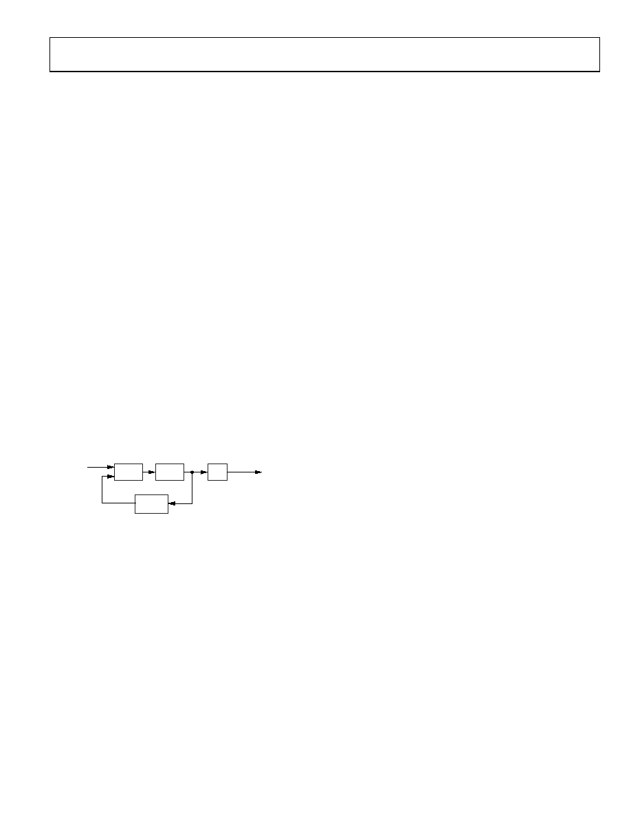
It is also important where the loop is closed. In this example,
the loop is closed before the output divider (see Figure 30).
fPFD
PFD
VCO
N
DIVIDER
÷2
RFOUT
09800-
027
Figure 30. Loop Closed Before Output Divider
Channel resolution (fRESOUT) of 200 kHz is required at the output
of the RF divider. Therefore, the channel resolution at the output
of the VCO (fRES) needs to be 2 × fRESOUT, that is, 400 kHz.
MOD = REFIN/fRES
MOD = 10 MHz/400 kHz = 25
From Equation 4,
fPFD = [10 MHz × (1 + 0)/1] = 10 MHz
(5)
2112.6 MHz = 10 MHz × [(INT + (FRAC/25))/2]
(6)
where:
INT = 422.
FRAC = 13.
REFERENCE DOUBLER AND REFERENCE DIVIDER
The on-chip reference doubler allows the input reference signal
to be doubled. Doubling the reference signal doubles the PFD
comparison frequency, which improves the noise performance of
the system. Doubling the PFD frequency usually improves noise
performance by 3 dB. Note that in fractional-N mode, the PFD
cannot operate above 32 MHz due to a limitation in the speed
of the Σ-Δ circuit of the N divider. For integer-N applications,
the PFD can operate up to 90 MHz.
The reference divide-by-2 divides the reference signal by 2,
resulting in a 50% duty cycle PFD frequency. This is necessary
for the correct operation of the cycle slip reduction (CSR)
function. For more information, see the Cycle Slip Reduction
for Faster Lock Times section.
12-BIT PROGRAMMABLE MODULUS
The choice of modulus (MOD) depends on the reference signal
(REFIN) available and the channel resolution (fRES) required at the
RF output. For example, a GSM system with 13 MHz REFIN sets
the modulus to 65. This means that the RF output resolution
(fRES) is the 200 kHz (13 MHz/65) necessary for GSM. With
dither off, the fractional spur interval depends on the selected
modulus values (see Table 7).
Unlike most other fractional-N PLLs, the ADF4351 allows the
user to program the modulus over a 12-bit range. When com-
bined with the reference doubler and the 10-bit R counter, the
12-bit modulus allows the user to set up the part in many
different configurations for the application.
For example, consider an application that requires a 1.75 GHz
RF frequency output with a 200 kHz channel step resolution.
The system has a 13 MHz reference signal.
One possible setup is to feed the 13 MHz reference signal
directly into the PFD and to program the modulus to divide
by 65. This results in the required 200 kHz resolution.
Another possible setup is to use the reference doubler to create
26 MHz from the 13 MHz input signal. The 26 MHz is then fed
into the PFD, and the modulus is programmed to divide by 130.
This setup also results in 200 kHz resolution but offers superior
phase noise performance over the first setup.
The programmable modulus is also very useful for multi-
standard applications. For example, if a dual-mode phone
requires PDC and GSM 1800 standards, the programmable
modulus is of great benefit.
PDC requires 25 kHz channel step resolution, whereas GSM 1800
requires 200 kHz channel step resolution. A 13 MHz reference
signal can be fed directly to the PFD, and the modulus can be
programmed to 520 when in PDC mode (13 MHz/520 = 25 kHz).
The modulus must be reprogrammed to 65 for GSM 1800 opera-
tion (13 MHz/65 = 200 kHz).
相关PDF资料 |
PDF描述 |
|---|---|
| GEM25DRYF | CONN EDGECARD 50POS DIP .156 SLD |
| GEM28DRTF | CONN EDGECARD 56POS DIP .156 SLD |
| H3AWH-4006G | IDC CABLE - HSC40H/AE40G/HPL40H |
| GEM28DRKF | CONN EDGECARD 56POS DIP .156 SLD |
| M1CXA-5036J | IDC CABLE - MKC50A/MC50G/X |
相关代理商/技术参数 |
参数描述 |
|---|---|
| EVAL-ADF4360-0EB1 | 制造商:AD 制造商全称:Analog Devices 功能描述:Integrated Synthesizer and VCO |
| EVAL-ADF4360-1EB1 | 制造商:Analog Devices 功能描述:Evaluation Board For ADF4360-1 |
| EVAL-ADF4360-1EBZ1 | 功能描述:BOARD EVALUATION FOR ADF4360-1 RoHS:是 类别:编程器,开发系统 >> 评估演示板和套件 系列:- 产品培训模块:Obsolescence Mitigation Program 标准包装:1 系列:- 主要目的:电源管理,电池充电器 嵌入式:否 已用 IC / 零件:MAX8903A 主要属性:1 芯锂离子电池 次要属性:状态 LED 已供物品:板 |
| EVAL-ADF4360-2EB1 | 制造商:Analog Devices 功能描述:EVALUATION BOARD FOR ADF4360-2 |
| EVAL-ADF4360-2EBZ1 | 功能描述:BOARD EVALUATION FOR ADF4360-2 RoHS:是 类别:编程器,开发系统 >> 评估演示板和套件 系列:- 标准包装:1 系列:PSoC® 主要目的:电源管理,热管理 嵌入式:- 已用 IC / 零件:- 主要属性:- 次要属性:- 已供物品:板,CD,电源 |
发布紧急采购,3分钟左右您将得到回复。