- 您现在的位置:买卖IC网 > PDF目录16863 > EVAL-ADF4360-2EBZ1 (Analog Devices Inc)BOARD EVALUATION FOR ADF4360-2 PDF资料下载
参数资料
| 型号: | EVAL-ADF4360-2EBZ1 |
| 厂商: | Analog Devices Inc |
| 文件页数: | 2/24页 |
| 文件大小: | 0K |
| 描述: | BOARD EVALUATION FOR ADF4360-2 |
| 标准包装: | 1 |
| 主要目的: | 计时,频率合成器 |
| 嵌入式: | 否 |
| 已用 IC / 零件: | ADF4360-2 |
| 主要属性: | 带 VCO 的单路整数-N PLL |
| 次要属性: | 2GHz,200kHz PFD |
| 已供物品: | 板,线缆,软件 |
| 相关产品: | ADF4360-2BCPZRL7-ND - IC SYNTHESIZER VCO 24LFCSP ADF4360-2BCPZRL-ND - IC SYNTHESIZER VCO 24LFCSP ADF4360-2BCPZ-ND - IC SYNTHESIZER/VCO 24-LFCSP |
ADF4360-2
Data Sheet
Rev. C | Page 10 of 24
MUXOUT AND LOCK DETECT
The output multiplexer on the ADF4360 family allows the user
to access various internal points on the chip. The state of
MUXOUT is controlled by M3, M2, and M1 in the function
latch. The full truth table is shown in Table 7. Figure 13 shows
the MUXOUT section in block diagram form.
Lock Detect
MUXOUT can be programmed for two types of lock detect:
digital and analog. Digital lock detect is active high. When LDP
in the R counter latch is set to 0, digital lock detect is set high
when the phase error on three consecutive phase detector cycles
is less than 15 ns.
With LDP set to 1, five consecutive cycles of less than 15 ns
phase error are required to set the lock detect. It stays set high
until a phase error of greater than 25 ns is detected on any
subsequent PD cycle.
The N-channel, open-drain, analog lock detect should be
operated with an external pull-up resistor of 10 k nominal.
When a lock is detected, the output is high with narrow low-
going pulses.
R COUNTER OUTPUT
N COUNTER OUTPUT
DIGITAL LOCK DETECT
DGND
CONTROL
MUX
MUXOUT
DVDD
ANALOG LOCK DETECT
SDOUT
04436-013
Figure 13. MUXOUT Circuit
INPUT SHIFT REGISTER
The ADF4360 family’s digital section includes a 24-bit input
shift register, a 14-bit R counter, and an 18-bit N counter
comprised of a 5-bit A counter and a 13-bit B counter. Data is
clocked into the 24-bit shift register on each rising edge of CLK.
The data is clocked in MSB first. Data is transferred from the
shift register to one of four latches on the rising edge of LE. The
destination latch is determined by the state of the two control
bits (C2, C1) in the shift register. The two LSBs are DB1 and
DB0, as shown in Figure 2.
a summary of how the latches are programmed. Note that the
test mode latch is used for factory testing and should not be
programmed by the user.
Table 5. C2 and C1 Truth Table
Control Bits
C2
C1
Data Latch
0
Control Latch
0
1
R Counter
1
0
N Counter (A and B)
1
Test Mode Latch
VCO
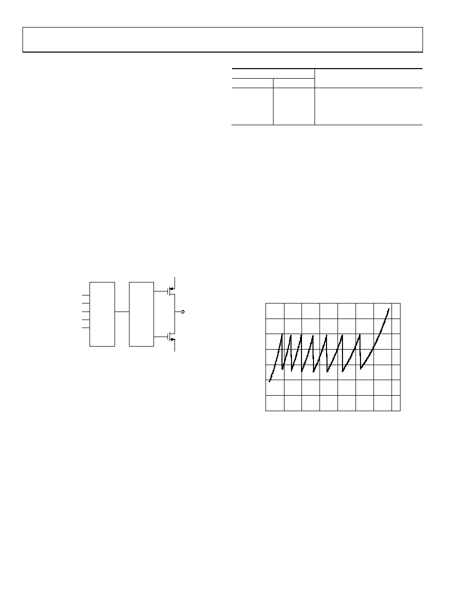
The VCO core in the ADF4360 family uses eight overlapping
bands, as shown in Figure 14, to allow a wide frequency range
to be covered without a large VCO sensitivity (KV) and resultant
poor phase noise and spurious performance.
The correct band is chosen automatically by the band select
logic at power-up or whenever the N counter latch is updated. It
is important that the correct write sequence be followed at
power-up. This sequence is
1. R counter latch
2. Control latch
3. N counter latch
During band select, which takes five PFD cycles, the VCO VTUNE
is disconnected from the output of the loop filter and is
connected to an internal reference voltage.
04436-014
1600
2300
2000
2100
2200
1900
1800
1700
FREQUENCY (MHz)
VOLTAGE
(V)
0
0.5
1.0
1.5
2.0
2.5
3.0
3.5
Figure 14. Frequency vs. VTUNE, ADF4360-2
The R counter output is used as the clock for the band select
logic and should not exceed 1 MHz. A programmable divider is
provided at the R counter input to allow division by 1, 2, 4, or 8
and is controlled by Bit BSC1 and Bit BSC2 in the R counter latch.
Where the required PFD frequency exceeds 1 MHz, the divide ratio
should be set to allow enough time for correct band selection.
After band selection, normal PLL action resumes. The nominal
value of KV is 57 MHz/V, or 28 MHz/V if divide-by-2 operation
is selected (by programming DIV2 [DB22] high in the N
counter latch). The ADF4360 family contains linearization
circuitry to minimize any variation of the product of ICP and KV.
相关PDF资料 |
PDF描述 |
|---|---|
| RBC10DRYS-S93 | CONN EDGECARD 20POS DIP .100 SLD |
| H0PPS-1018M | DIP CABLE - HDP10S/AE10M/HDP10S |
| RNF-100-1-1/2-BK-STK | HEATSHRINK RNF-100 1 1/2"X4' BLK |
| UBT1J220MPD1TD | CAP ALUM 22UF 63V 20% RADIAL |
| V110B24E150BL2 | CONVERTER MOD DC/DC 24V 150W |
相关代理商/技术参数 |
参数描述 |
|---|---|
| EVAL-ADF4360-3EB1 | 制造商:Analog Devices 功能描述:EVALUATION BOARD FOR ADF4360-3 |
| EVAL-ADF4360-4EB1 | 制造商:AD 制造商全称:Analog Devices 功能描述:Integrated Synthesizer and VCO |
| EVAL-ADF4360-4EBZ1 | 制造商:Analog Devices 功能描述:Evaluation Board Integrated Synthesizer And VCO 制造商:Analog Devices 功能描述:Evaluation Board I.C. |
| EVAL-ADF4360-5EB1 | 制造商:Analog Devices 功能描述:EVALUATION BOARD FOR ADF4360-5 |
| EVAL-ADF4360-5EBZ1 | 制造商:Analog Devices 功能描述: |
发布紧急采购,3分钟左右您将得到回复。