- 您现在的位置:买卖IC网 > PDF目录16863 > EVAL-ADF4360-2EBZ1 (Analog Devices Inc)BOARD EVALUATION FOR ADF4360-2 PDF资料下载
参数资料
| 型号: | EVAL-ADF4360-2EBZ1 |
| 厂商: | Analog Devices Inc |
| 文件页数: | 8/24页 |
| 文件大小: | 0K |
| 描述: | BOARD EVALUATION FOR ADF4360-2 |
| 标准包装: | 1 |
| 主要目的: | 计时,频率合成器 |
| 嵌入式: | 否 |
| 已用 IC / 零件: | ADF4360-2 |
| 主要属性: | 带 VCO 的单路整数-N PLL |
| 次要属性: | 2GHz,200kHz PFD |
| 已供物品: | 板,线缆,软件 |
| 相关产品: | ADF4360-2BCPZRL7-ND - IC SYNTHESIZER VCO 24LFCSP ADF4360-2BCPZRL-ND - IC SYNTHESIZER VCO 24LFCSP ADF4360-2BCPZ-ND - IC SYNTHESIZER/VCO 24-LFCSP |
ADF4360-2
Data Sheet
Rev. C | Page 16 of 24
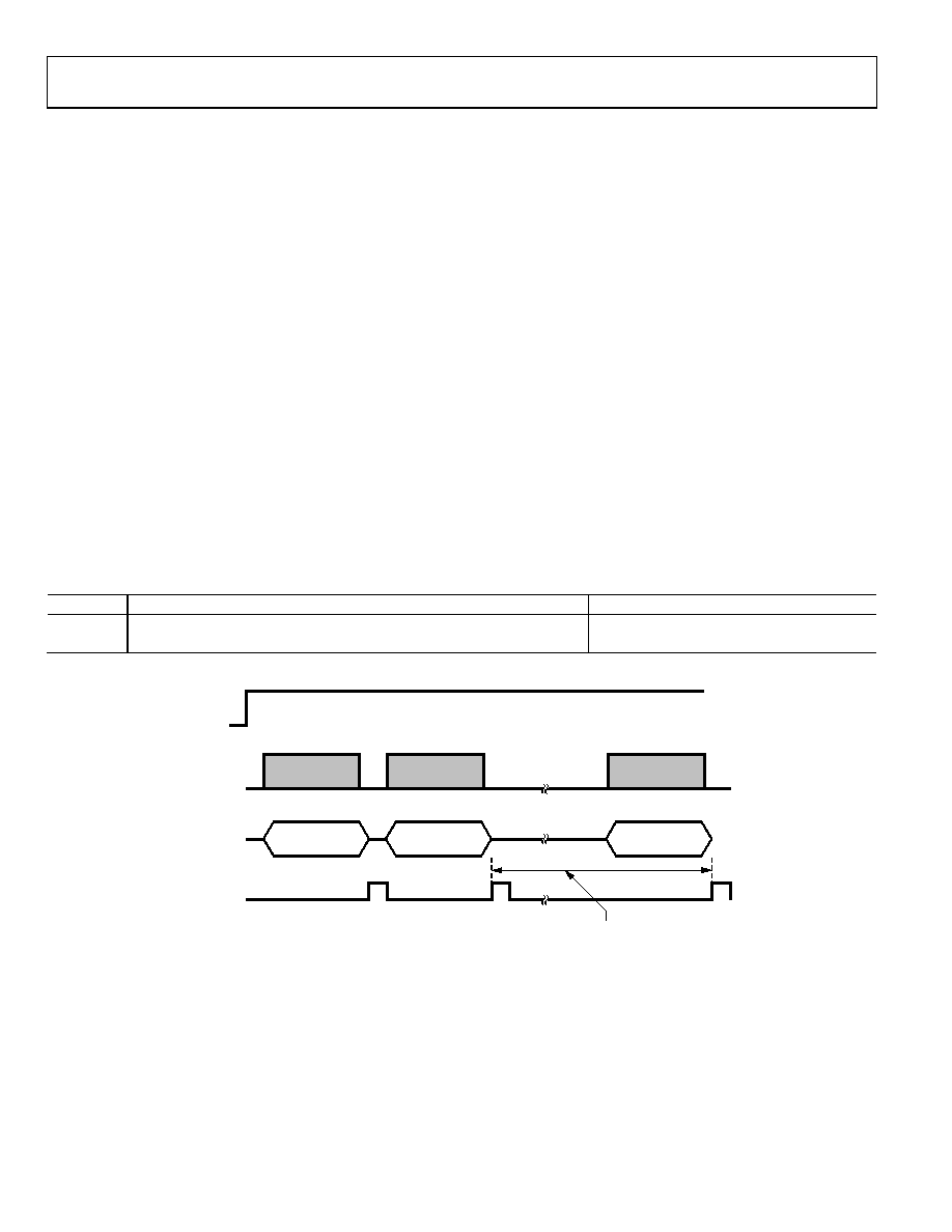
POWER-UP
Power-Up Sequence
The correct programming sequence for the ADF4360-2 after
power-up is as:
1. R counter latch
2. Control latch
3. N counter latch
Initial Power-Up
Initial power-up refers to programming the part after the
application of voltage to the AVDD, DVDD, VVCO, and CE pins. On
initial power-up, an interval is required between programming
the control latch and programming the N counter latch.
This interval is necessary to allow the transient behavior of the
ADF4360-2 during initial power-up to have settled. During
initial power-up, a write to the control latch powers up the part
and the bias currents of the VCO begin to settle. If these
currents have not settled to within 10% of their steady-state
value, and if the N counter latch is then programmed, the VCO
may not be able to oscillate at the desired frequency, which does
not allow the band select logic to choose the correct frequency
band and the ADF4360-2 may not achieve lock. If the
recommended interval is inserted and the N counter latch is
programmed, the band select logic can choose the correct
frequency band, and the part locks to the correct frequency.
The duration of this interval is affected by the value of the
capacitor on the CN pin (Pin 14). This capacitor is used to
reduce the close-in noise of the ADF4360-2 VCO. The
recommended value of this capacitor is 10 F. Using this value
requires an interval of ≥ 5 ms between the latching in of the
control latch bits and the latching in of the N counter latch bits.
If a shorter delay is required, this capacitor can be reduced. A
slight phase noise penalty is incurred by this change, which is
explained further in Table 10.
Table 10. CN Capacitance vs. Interval and Phase Noise
CN Value
Recommended Interval Between Control Latch and N Counter Latch
Open-Loop Phase Noise @ 10 kHz Offset
10 F
≥ 5 ms
86 dBc
440 nF
≥ 600 s
85 dBc
CLOCK
POWER-UP
DATA
LE
R COUNTER
LATCH DATA
CONTROL
LATCH DATA
N COUNTER
LATCH DATA
REQUIRED INTERVAL
CONTROL LATCH WRITE TO
N COUNTER LATCH WRITE
04436-020
Figure 16. ADF4360-2 Power-Up Timing
相关PDF资料 |
PDF描述 |
|---|---|
| RBC10DRYS-S93 | CONN EDGECARD 20POS DIP .100 SLD |
| H0PPS-1018M | DIP CABLE - HDP10S/AE10M/HDP10S |
| RNF-100-1-1/2-BK-STK | HEATSHRINK RNF-100 1 1/2"X4' BLK |
| UBT1J220MPD1TD | CAP ALUM 22UF 63V 20% RADIAL |
| V110B24E150BL2 | CONVERTER MOD DC/DC 24V 150W |
相关代理商/技术参数 |
参数描述 |
|---|---|
| EVAL-ADF4360-3EB1 | 制造商:Analog Devices 功能描述:EVALUATION BOARD FOR ADF4360-3 |
| EVAL-ADF4360-4EB1 | 制造商:AD 制造商全称:Analog Devices 功能描述:Integrated Synthesizer and VCO |
| EVAL-ADF4360-4EBZ1 | 制造商:Analog Devices 功能描述:Evaluation Board Integrated Synthesizer And VCO 制造商:Analog Devices 功能描述:Evaluation Board I.C. |
| EVAL-ADF4360-5EB1 | 制造商:Analog Devices 功能描述:EVALUATION BOARD FOR ADF4360-5 |
| EVAL-ADF4360-5EBZ1 | 制造商:Analog Devices 功能描述: |
发布紧急采购,3分钟左右您将得到回复。