- 您现在的位置:买卖IC网 > PDF目录97935 > EVB3020A-IFBD GSM Multiband RF Transceiver PDF资料下载
参数资料
| 型号: | EVB3020A-IFBD |
| 英文描述: | GSM Multiband RF Transceiver |
| 中文描述: | 手机多频段射频收发器 |
| 文件页数: | 19/44页 |
| 文件大小: | 409K |
| 代理商: | EVB3020A-IFBD |
第1页第2页第3页第4页第5页第6页第7页第8页第9页第10页第11页第12页第13页第14页第15页第16页第17页第18页当前第19页第20页第21页第22页第23页第24页第25页第26页第27页第28页第29页第30页第31页第32页第33页第34页第35页第36页第37页第38页第39页第40页第41页第42页第43页第44页
Advance Data Sheet
W3020 GSM Multiband RF Transceiver
December 1999
26
Lucent Technologies Inc.
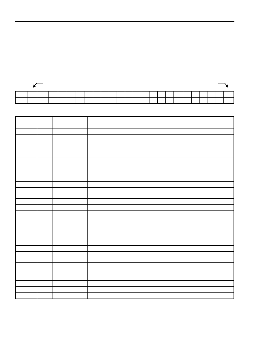
Programming Information (continued)
CONFIG Register
The CONFIG register contains bits to control various options for dc offset correction, filter-tuning, lock detect,
and overload outputs, etc. It is expected that this register would be written once at initialization and then rarely
updated. Since it is not affected by the power-on reset circuit, a write to this register should be the first operation
performed when accessing the W3020 chip. Also, it is advisable never to update the configuration register while
a critical operation is in progress.
Last bit in serial sequence
First bit in serial sequence
Bit No.
1
2
3
4
5
6
7
8
9
10
11
12
13
14
15
16
17
18
19
20
21
22
23
24
Bit
A0=1 A1=0
RS
DT0 DT1 DT2 C1
C2
C3
C4
C5
C6
C7 LD2 C8
VO
C9 OLD C10 F1
F2
F3
F4 A2=1
Table 27. CONFIG Register
Bit No.
Bit
SC1 Standard
Setting
Function
24
A2
1
Address Bit 2
23
22
21
20
F4
F3
F2
F1
0
Reserved
19
C10
1
Enable of LO2 PLL (See Table 28.)
18
OLD
0
Disable of Overload Pin Output Signal, When High (See Table 29.)
17
C9
0
Force RF Mixer On When RX LO1 Buffer Is On, When High (See
Table 30.)
16
VO
1
Reserved; Always High (See Table 31.)
15
C8
0
LO2 Charge Pump Output Off (high impedance), When High (See
Table 32.)
14
LD2
1
Enable LO2 Lock Detect Output, When High (See Table 33.)
13
C7
0
Select dc Offset Correction/Fine Tune, When High (See Table 34.)
12
C6
0
Disable LP Filter Bandwidth Tune and Use Default Value, When High
(See Table 35.)
11
C5
0
Disable dc Offset Correction and Use Default Setting, When High (See
Table 36.)
10
C4
1
High Bandwidth Setting of Baseband Path, When High (See Table 37.)
9
C3
0
RX LO1 Buffer On During dc Calibration When High (See Table 38.)
8
C2
0
LNA On During dc Calibration, When High (See Table 39.)
7
C1
1
LO2 Phase Detector Polarity, Positive Slope, When High (See
Table 40.)
6
5
4
DT[2]
DT[1]
DT[0]
0
1
dc Offset Correction Time (See Table 41.)
3
RS
1*
Resets Bit Content in Other Registers, When High (See Table 42.)
2
A1
0
Address Bit 1
1
A0
1
Address Bit 0
* It is recommended that a reset be programmed after power-on. Reset does not affect the content of the CONFIG register.
相关PDF资料 |
PDF描述 |
|---|---|
| EVB3030A | W3030 3 V Dual-Mode IF Cellular Receiver |
| EVB72001 | EVB72001 EValuation board for TH72001 |
| EVB72002 | EVB72002 EValuation Board for TH72002 |
| EVB72011 | EVB72011 EValuation Board for TH72011 |
| EVB72012 | EVB72012 EValuation Board for TH72012 |
相关代理商/技术参数 |
参数描述 |
|---|---|
| EVB3030A | 制造商:AGERE 制造商全称:AGERE 功能描述:W3030 3 V Dual-Mode IF Cellular Receiver |
| EVB-3250 | 功能描述:界面开发工具 Evaluation Board RoHS:否 制造商:Bourns 产品:Evaluation Boards 类型:RS-485 工具用于评估:ADM3485E 接口类型:RS-485 工作电源电压:3.3 V |
| EVB32-M8L | 制造商:Leviton Manufacturing Co 功能描述: |
| EVB-3300 | 功能描述:界面开发工具 USB3300 Hi-Speed USB Phy Evaluation Board RoHS:否 制造商:Bourns 产品:Evaluation Boards 类型:RS-485 工具用于评估:ADM3485E 接口类型:RS-485 工作电源电压:3.3 V |
| EVB-3500 | 功能描述:界面开发工具 Evaluation Board RoHS:否 制造商:Bourns 产品:Evaluation Boards 类型:RS-485 工具用于评估:ADM3485E 接口类型:RS-485 工作电源电压:3.3 V |
发布紧急采购,3分钟左右您将得到回复。