参数资料
| 型号: | EX128-FTQG64 |
| 厂商: | Microsemi SoC |
| 文件页数: | 44/48页 |
| 文件大小: | 0K |
| 描述: | IC FPGA ANTIFUSE 6K 64-TQFP |
| 标准包装: | 160 |
| 系列: | EX |
| 逻辑元件/单元数: | 256 |
| 输入/输出数: | 46 |
| 门数: | 6000 |
| 电源电压: | 2.3 V ~ 2.7 V |
| 安装类型: | 表面贴装 |
| 工作温度: | 0°C ~ 70°C |
| 封装/外壳: | 64-LQFP |
| 供应商设备封装: | 64-TQFP(10x10) |
第1页第2页第3页第4页第5页第6页第7页第8页第9页第10页第11页第12页第13页第14页第15页第16页第17页第18页第19页第20页第21页第22页第23页第24页第25页第26页第27页第28页第29页第30页第31页第32页第33页第34页第35页第36页第37页第38页第39页第40页第41页第42页第43页当前第44页第45页第46页第47页第48页
Revision 10
1-1
1 – eX FPGA Architecture and Characteristics
General Description
The eX family of FPGAs is a low-cost solution for low-power, high-performance designs. The inherent
low power attributes of the antifuse technology, coupled with an additional low static power mode, make
these devices ideal for power-sensitive applications. Fabricated with an advanced 0.22 mm CMOS
antifuse technology, these devices achieve high performance with no power penalty.
eX Family Architecture
Microsemi eX family is implemented on a high-voltage twin-well CMOS process using 0.22 m design
rules. The eX family architecture uses a “sea-of-modules” structure where the entire floor of the device is
covered with a grid of logic modules with virtually no chip area lost to interconnect elements or routing.
Interconnection among these logic modules is achieved using Microsemi patented metal-to-metal
programmable antifuse interconnect elements. The antifuse interconnect is made up of a combination of
amorphous silicon and dielectric material with barrier metals and has an "on" state resistance of 25
with
a capacitance of 1.0fF for low-signal impedance. The antifuses are normally open circuit and, when
programmed, form a permanent low-impedance connection. The eX family provides two types of logic
modules, the register cell (R-cell) and the combinatorial cell (C-cell).
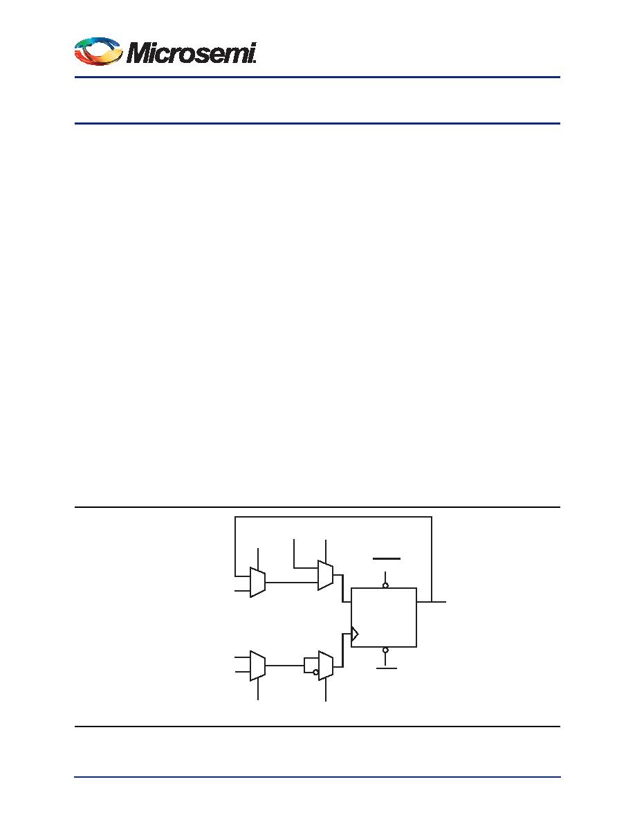
The R-cell contains a flip-flop featuring asynchronous clear, asynchronous preset, and clock enable
(using the S0 and S1 lines) control signals (Figure 1-1). The R-cell registers feature programmable clock
polarity selectable on a register-by-register basis. This provides additional flexibility while allowing
mapping of synthesized functions into the eX FPGA. The clock source for the R-cell can be chosen from
either the hard-wired clock or the routed clock.
The C-cell implements a range of combinatorial functions up to five inputs (Figure 1-2 on page 1-2).
Inclusion of the DB input and its associated inverter function enables the implementation of more than
4,000 combinatorial functions in the eX architecture in a single module.
Two C-cells can be combined together to create a flip-flop to imitate an R-cell via the use of the CC
macro. This is particularly useful when implementing non-timing-critical paths and when the design
engineer is running out of R-cells. More information about the CC macro can be found in the Maximizing
Logic Utilization in eX, SX and SX-A FPGA Devices Using CC Macros application note.
Figure 1-1 R-Cell
DirectConnect
Input
CLKA,
CLKB,
Internal Logic
HCLK
CKS
CKP
CLR
PSET
Y
DQ
Routed
Data Input
S0
S1
相关PDF资料 |
PDF描述 |
|---|---|
| EX64-PTQ64 | IC FPGA ANTIFUSE 3K 64-TQFP |
| ACM43DRTN-S13 | CONN EDGECARD EXTEND 86POS 0.156 |
| ABM43DRTN-S13 | CONN EDGECARD EXTEND 86POS .156 |
| BR25L010FJ-WE2 | IC EEPROM 1KBIT 5MHZ 8SOP |
| ACM43DRTH-S13 | CONN EDGECARD EXTEND 86POS 0.156 |
相关代理商/技术参数 |
参数描述 |
|---|---|
| EX128-PCS100 | 制造商:未知厂家 制造商全称:未知厂家 功能描述:eX Family FPGAs |
| EX128-PCS100A | 制造商:ACTEL 制造商全称:Actel Corporation 功能描述:eX Family FPGAs |
| EX128-PCS100I | 制造商:未知厂家 制造商全称:未知厂家 功能描述:eX Family FPGAs |
| EX128-PCS100PP | 制造商:未知厂家 制造商全称:未知厂家 功能描述:eX Family FPGAs |
| EX128-PCS128 | 制造商:未知厂家 制造商全称:未知厂家 功能描述:eX Family FPGAs |
发布紧急采购,3分钟左右您将得到回复。