- 您现在的位置:买卖IC网 > PDF目录68993 > FA5502P (FUJI ELECTRIC CO LTD) 1.5 A POWER FACTOR CONTROLLER, 150 kHz SWITCHING FREQ-MAX, PDIP16 PDF资料下载
参数资料
| 型号: | FA5502P |
| 厂商: | FUJI ELECTRIC CO LTD |
| 元件分类: | 稳压器 |
| 英文描述: | 1.5 A POWER FACTOR CONTROLLER, 150 kHz SWITCHING FREQ-MAX, PDIP16 |
| 封装: | DIP-16 |
| 文件页数: | 8/23页 |
| 文件大小: | 217K |
| 代理商: | FA5502P |
16
Quality is our message
FA5502P/M
(6) ON/OFF control circuit
Fig.12 shows the configuration of the ON/OFF
control circuit. The ON/OFF control circuit consists of a
comparator with hysteresis. To turn the IC from OFF
mode to operating mode, pull up the ON/OFF pin
voltage to 3.95V (typ.) or higher. On the other hand, to
turn the IC from operating mode to OFF mode, pull
down the ON/OFF pin to 2.80V (typ.) or lower.
In the OFF mode, the reference (REF) voltage is cut
off, and the CS pin and OUT pin go approximately 0V.
IC consumption current during OFF mode is 200A
(max.) which is much smaller than at an operating
mode.
The input current at ON/OFF pin is a very small
value of 500nA.
In the case that external signal is applied to ON/OFF
pin, the ON/OFF pin voltage must not exceed the VCC
pin voltage, even when start up or stop operation.
If ON/OFF operation is not made by external signal,
the ON/OFF pin is normally pulled up to Vcc pin
through 10k
to 1M. Then ON/OFF pin voltage goes
to approximately Vcc voltage.
12
REF circuit
Output circuit
ON/OFF
3.95/2.80V
Fig.12 ON/OFF control circuit
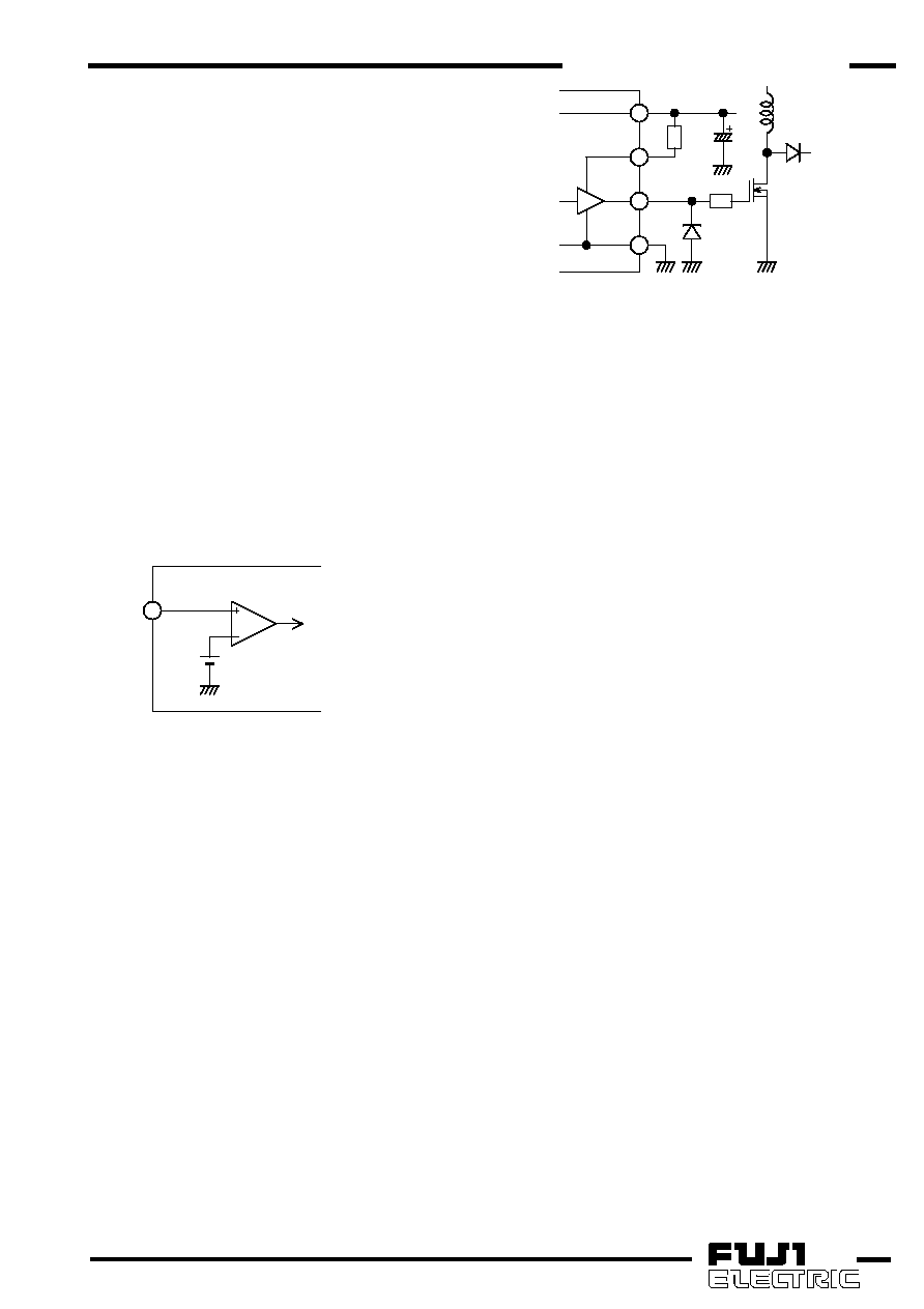
(7) Output circuit
As shown in Fig.13, VC pin (pin 9) is configured as
the high power terminal, independent of the IC power
terminal (VCC pin). This pin allows an independent
drive resistance when the power MOSFET is ON and
OFF. Suppose the drive resistance when ON and OFF
are Rg (on) and Rg (off),
Rg(on)=Rg1+Rg2 (9)
Rg(off)=Rg2 (10)
At standby, the OUT pin is kept Low.
If the drain voltage of power MOSFET oscillates, a
parasitic capacitance between gate and drain may
swing the OUT pin (pin 8) of IC below 0V. If OUT pin
voltage falls below -0.3V, a current may flow to the
parasitic element in IC, whereby the IC may
malfunction. In such a case, Schottky diode must be
connected between OUT pin and GND so as not to
allow a parasitic current to flow to IC.
If VC pin is fed with a source which is independent
of VCC pin, the voltage of VC pin must not exceed that
of VCC pin even start up or stop operation.
8
9
7
10
Rg1
C5
Rg2
Shottky
diode
GND
OUT
VC
VCC
Fig.13 Output circuit
(8) Undervoltage lockout circuit
This IC contains an undervoltage lockout circuit to
prevent malfunction when the Vcc voltage drops.
When the Vcc voltage rises from 0V, this IC starts
operation at 16.5V (typ.). If the Vcc voltage drops after
the IC starts up, this IC stops operation at 8.9V(typ.).
When IC stops operation by undervoltage lockout
circuit, OUT pin and CS pin is kept low
(9) Compensation circuit for light load
If the output of multiplier and the input of current
error amplifier do not have offset voltage, the input
current to the converter is approximately zero under
condition that the PFC converter operates in no load.
But an actual multiplier and current error amplifier may
have offset voltage. If the offset voltage is negative,
the input current, which corresponds to the offset
voltage, flows into the converter even when the PFC
converter operates in no load. In this case, the PFC
output voltage rises abnormally because of too much
input current.
To avoid these, this IC has an automatic offset
correction circuit for light load. The output voltage of
error amplifier is approximately 1.55V or higher in
normal operation.
If the output voltage drops below 1.55V, this circuit
operates. If there is a negative offset voltage, the
output voltage of error amplifier falls below 1.55V in
the case that the PFC converter operates in no load or
light load. Then, the offset voltage is corrected in the
multiplier circuit. Because of this operation, even
under no load or light load, the PFC output voltage
does not rise abnormally, but is always kept stable.
The amount of correction changes linearly according
to the output of error amplifier, which can make
operation stable.
Fig.14 shows the outline of the effect of this circuit.
相关PDF资料 |
PDF描述 |
|---|---|
| FA5515P | 1.5 A SWITCHING CONTROLLER, 500 kHz SWITCHING FREQ-MAX, PDIP8 |
| FA5514N | 1.5 A SWITCHING CONTROLLER, 500 kHz SWITCHING FREQ-MAX, PDSO8 |
| FA5515N | 1.5 A SWITCHING CONTROLLER, 500 kHz SWITCHING FREQ-MAX, PDSO8 |
| FA5510N | 1.5 A SWITCHING CONTROLLER, 500 kHz SWITCHING FREQ-MAX, PDSO8 |
| FA5511P | 1.5 A SWITCHING CONTROLLER, 500 kHz SWITCHING FREQ-MAX, PDIP8 |
相关代理商/技术参数 |
参数描述 |
|---|---|
| FA5502P/M | 制造商:未知厂家 制造商全称:未知厂家 功能描述:FA5502P/M is a control IC for a power factor correction system. |
| FA5502P-A2 | 制造商:Fuji Electric 功能描述: |
| FA5504P-D1 | 制造商:Fuji Electric 功能描述: |
| FA551 | 制造商:Black Box Corporation 功能描述:TRANSCEIVER CONNECTOR KITFEMAL |
| FA5510N | 制造商:未知厂家 制造商全称:未知厂家 功能描述:CMOS IC For Switching Power Supply Control |
发布紧急采购,3分钟左右您将得到回复。