- 您现在的位置:买卖IC网 > PDF目录67412 > FA7703V (FUJI ELECTRIC CO LTD) 0.4 A DUAL SWITCHING CONTROLLER, 1000 kHz SWITCHING FREQ-MAX, PDSO16 PDF资料下载
参数资料
| 型号: | FA7703V |
| 厂商: | FUJI ELECTRIC CO LTD |
| 元件分类: | 稳压器 |
| 英文描述: | 0.4 A DUAL SWITCHING CONTROLLER, 1000 kHz SWITCHING FREQ-MAX, PDSO16 |
| 封装: | 1.10 MM, TSSOP-16 |
| 文件页数: | 9/21页 |
| 文件大小: | 242K |
| 代理商: | FA7703V |
17
Quality is our message
FA7703/04
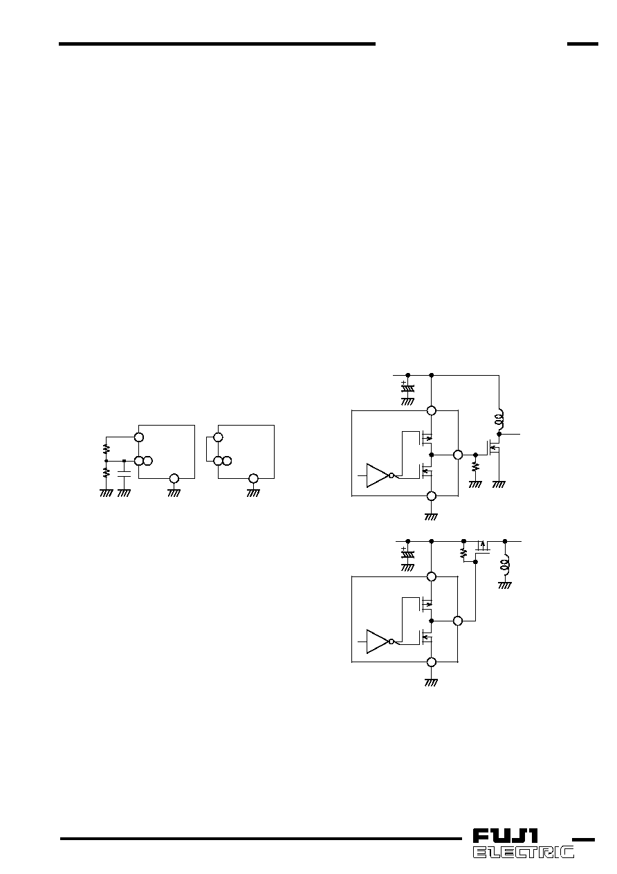
(4)Setting the maximum output duty
If you need to control the maximum output duty
in the DC-DC converter circuit, you can control
pulse width by connecting REG terminal to DT
terminal divided with resistors R5 and R6, as
described in Fig. 9. The output duty of the
voltage of DT terminal in this case changes
according
to
the
operation
frequency,
as
described in the chart of “DT terminal voltage vs.
output duty cycle” characteristic curves. Set the
output duty accordingly based on your required
operation frequency. If the maximum output duty
setting is not needed, be sure to connect DT
terminal directly to REG terminal. In this case,
the pulse width widens up to the output duty of
100%.
The voltage of DT terminal should be set in the
range of 0.65V to 1.1V(typ.). There is a
possibility of distortion of the output pulses if
strong noises or the like are applied to DT
terminal. When conducting pattern wiring, do it
as close to each terminal of the IC as possible.
Besides, it is strongly recommended to connect
a capacitor CDT for a filter of noise prevention.
(5)Pull-up/Pull-down resistor at the output
section
The power source of FA7703/04 to control the
output section is supplied from the voltage of
VREG, the voltage of this power source is
accordingly not stationary below the UVLO
voltage. On the other hand, OUT terminal
becomes unsteady condition while Power supply
voltage is below UVLO voltage. Be sure to
connect a pull-up resistor/pull-down resistor
according to Fig. 10. (See Fig. 10)
(6)Restriction
of
external
discrete
components/Recommended
operating
conditions
To achieve a stable operation of FA7703/04, the
values
of
external
discrete
components
connected to VCC, REF, and CS terminals of
this
IC
should
be
within
the
range
of
recommended operating conditions. And also
the voltage and the current applied to each
terminal should be within the recommended
operating conditions.
A Pch MOSFET is installed between VCC
terminal and OUT1 terminal, and between VCC
terminal and OUT2 terminal. Since the Pch
MOSFET has a parasitic diode, if the voltage of
OUT1 and OUT2 terminals becomes higher than
the VCC terminal voltage, the current flows from
each terminal to VCC terminal. Cautious care
must be taken accordingly when designing.
10
9
7
Vcc
GND
OUT1
VIN
8
9
7
Vcc
GND
OUT2
VIN
Fig.10
Fig.9
3 15
16
7
REG
DT1 or DT2
GND
R5
R6
CDT
3 15
16
7
REG
DT1 or DT2
GND
setting
maximum
Duty cycle
Not needed
maximum Duty
cycle
相关PDF资料 |
PDF描述 |
|---|---|
| FA7704M | 0.4 A DUAL SWITCHING CONTROLLER, 1000 kHz SWITCHING FREQ-MAX, PDSO16 |
| FA7703M | 0.4 A DUAL SWITCHING CONTROLLER, 1000 kHz SWITCHING FREQ-MAX, PDSO16 |
| FA7738N | 5.5 A SWITCHING REGULATOR, 400 kHz SWITCHING FREQ-MAX, PDSO8 |
| FA7738P | 5.5 A SWITCHING REGULATOR, 400 kHz SWITCHING FREQ-MAX, PDIP8 |
| FAB2200UCX | 1.2 W, 2 CHANNEL, AUDIO AMPLIFIER, PBGA25 |
相关代理商/技术参数 |
参数描述 |
|---|---|
| FA7704 | 制造商:FUJI 制造商全称:Fuji Electric 功能描述:FUJI Power Supply Control IC |
| FA771 | 制造商:Black Box Corporation 功能描述:DB25 TO RJ45,8 WIRE,F MOD THUMBSCREW ADPTR KIT |
| FA7711V | 制造商:FUJI 制造商全称:Fuji Electric 功能描述:FUJI Power Supply Control IC |
| FA7726 | 制造商:FUJI 制造商全称:Fuji Electric 功能描述:45V Input Buck Converter 3ch/2ch IC with Power MOSFET |
| FA7730 | 制造商:FUJI 制造商全称:Fuji Electric 功能描述:45V Input Buck Converter 3ch/2ch IC with Power MOSFET |
发布紧急采购,3分钟左右您将得到回复。