- 您现在的位置:买卖IC网 > PDF目录67412 > FAN5061M (FAIRCHILD SEMICONDUCTOR CORP) SWITCHING CONTROLLER, 345 kHz SWITCHING FREQ-MAX, PDSO20 PDF资料下载
参数资料
| 型号: | FAN5061M |
| 厂商: | FAIRCHILD SEMICONDUCTOR CORP |
| 元件分类: | 稳压器 |
| 英文描述: | SWITCHING CONTROLLER, 345 kHz SWITCHING FREQ-MAX, PDSO20 |
| 封装: | SOIC-20 |
| 文件页数: | 4/18页 |
| 文件大小: | 149K |
| 代理商: | FAN5061M |
FAN5061
12
Pr
eliminar
y
Specication
Application Circuit Summary
Table 4 summarizes the worst-case design schematics presented in this section. The basic choices are: A) The processor, B) the
chipset used, and C) the use or not of a sense resistor. Depending on board layout and component selection, it may be possible to
use fewer output capacitors than shown here. For congurations not shown in this datasheet, consult the Appendix for selection
of component values.
Table 4. Recommended Values for CPU-based Applications
*Output capacitance requirements depend critically on layout and processor type. Consult Application Bulletin AB-14 for details.
See the Appendix to this datasheet for the method of calculation of these components. Pin 4 must be used to remote sense the
voltage at the processor to achieve the specified performance.
Processor
Chipset
CIN
COUT*
R5, R7 (K
)
Coppermine
Whitney
3
4
8.45
Katmai
Camino
4
6
13.0
Mendocino
Whitney
4
5
11.3
Katmai
BX
5
6
11.8
Test Parameters
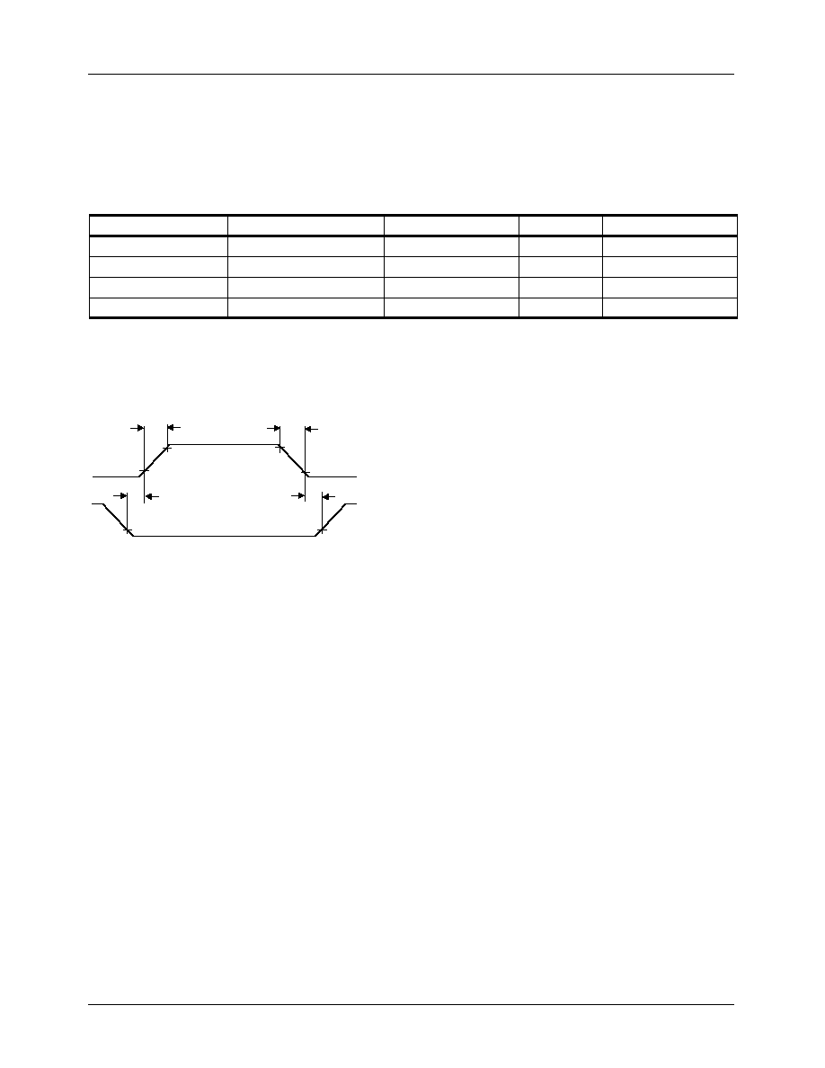
Figure 3. Ouput Drive Timing Diagram
Application Information
The FAN5061 Controller
The FAN5061 is a programmable synchronous DC-DC con-
troller IC. When designed around the appropriate external
components, the FAN5061 can be congured to deliver more
than 16A of output current, as appropriate for the Katmai and
Coppermine and other processors. The FAN5061 functions
as a xed frequency PWM step down regulator.
Main Control Loop
Refer to the FAN5061 Block Diagram on page 1. The FAN5061
implements “summing mode control”, which is different from
both classical voltage-mode and current-mode control. It
provides superior performance to either by allowing a large
converter bandwidth over a wide range of output loads.
The control loop of the regulator contains two main sections:
the analog control block and the digital control block. The
analog section consists of signal conditioning ampliers feeding
into a comparator which provides the input to the digital control
block. The signal conditioning section accepts input from the
DROOP (current feedback) and VFB (voltage feedback) pins
and sets up two controlling signal paths. The rst, the voltage
control path, amplies the difference between the VFB signal
and the reference voltage from the DAC and presents the
output to one of the summing amplier inputs. The second,
current control path, takes the difference between the DROOP
and SW pins when the high-side MOSFET is on, reproducing
the voltage across the MOSFET and thus the input current; it
presents the resulting signal to another input of the summing
amplier. These two signals are then summed together. This
output is then presented to a comparator looking at the oscillator
ramp, which provides the main PWM control signal to the
digital control block.
The digital control block takes the analog comparator input
and the main clock signal from the oscillator to provide the
appropriate pulses to the HIDRV and LODRV output pins.
These two outputs control the external power MOSFETs.
There is an additional comparator in the analog control section
whose function is to set the point at which the FAN5061 cur-
rent limit comparator disables the output drive signals to the
external power MOSFETs.
High Current Output Drivers
The FAN5061 contains two identical high current output driv-
ers that utilize high speed bipolar transistors in a push-pull
conguration. The drivers’ power and ground are separated
from the chip’s power and ground for switching noise immu-
nity. The power supply pin, VCCP, is supplied from an exter-
nal 12V source through a series 33
resistor. The resulting
voltage is sufcient to provide the gate to source drive to the
external MOSFETs required in order to achieve a low RDS,ON.
Internal Voltage Reference
The reference included in the FAN5061 is a precision band-gap
voltage reference. Its internal resistors are precisely trimmed
to provide a near zero temperature coefcient (TC). Based on
the reference is the output from an integrated 5-bit DAC. The
DAC monitors the 5 voltage identication pins, VID0-4. When
the VID4 pin is at logic HIGH, the DAC scales the reference
voltage from 2.0V to 3.5V in 100mV increments. When VID4
tR
5V
tDT
tF
HIDRV
to SW
LODRV
2V
5V
2V
相关PDF资料 |
PDF描述 |
|---|---|
| FAN5201MSA | 6 A BATTERY CHARGE CONTROLLER, 275 kHz SWITCHING FREQ-MAX, PDSO24 |
| FAN5361UMP10X | SWITCHING REGULATOR, DSO6 |
| FAN5361UC13X | SWITCHING REGULATOR, PBGA6 |
| FAN5361UC15X | SWITCHING REGULATOR, PBGA6 |
| FAN5361UMP12X | SWITCHING REGULATOR, DSO6 |
相关代理商/技术参数 |
参数描述 |
|---|---|
| FAN5063 | 制造商:FAIRCHILD 制造商全称:Fairchild Semiconductor 功能描述:ACPI Dual Switch Controller |
| FAN5063A WAF | 制造商:Fairchild Semiconductor Corporation 功能描述: |
| FAN5063M | 功能描述:开关变换器、稳压器与控制器 aCPI Dual Switch Controller RoHS:否 制造商:Texas Instruments 输出电压:1.2 V to 10 V 输出电流:300 mA 输出功率: 输入电压:3 V to 17 V 开关频率:1 MHz 工作温度范围: 安装风格:SMD/SMT 封装 / 箱体:WSON-8 封装:Reel |
| FAN5063MX | 功能描述:开关变换器、稳压器与控制器 aCPI Dual Switch Controller RoHS:否 制造商:Texas Instruments 输出电压:1.2 V to 10 V 输出电流:300 mA 输出功率: 输入电压:3 V to 17 V 开关频率:1 MHz 工作温度范围: 安装风格:SMD/SMT 封装 / 箱体:WSON-8 封装:Reel |
| FAN5063-ZCA3026B WAF | 制造商:Fairchild Semiconductor Corporation 功能描述: |
发布紧急采购,3分钟左右您将得到回复。