- 您现在的位置:买卖IC网 > PDF目录172369 > FAN5094MTC (FAIRCHILD SEMICONDUCTOR CORP) PDF资料下载
参数资料
| 型号: | FAN5094MTC |
| 厂商: | FAIRCHILD SEMICONDUCTOR CORP |
| 元件分类: | 稳压器 |
| 中文描述: | 3 A SWITCHING CONTROLLER, 2000 kHz SWITCHING FREQ-MAX, PDSO28 |
| 封装: | TSSOP-28 |
| 文件页数: | 16/22页 |
| 文件大小: | 182K |
| 代理商: | FAN5094MTC |
PRODUCT SPECIFICATION
FAN5094
REV. 1.0.2 5/13/02
3
Absolute Maximum Ratings
19
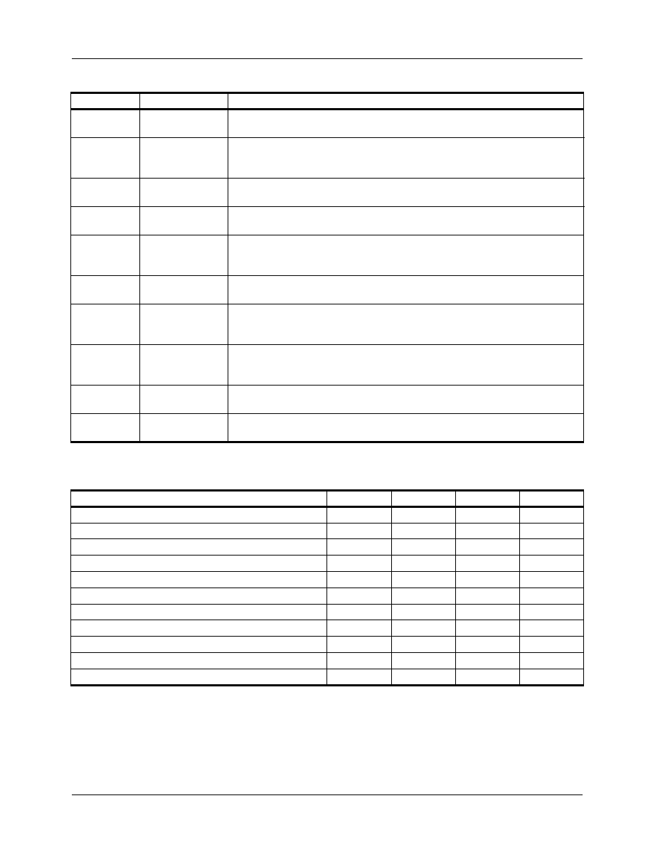
GNDA
Ground A. Ground-side current sense pin. Connect directly to low-side
MOSFET source, or to sense resistor ground.
20
LDRVA
Low Side FET Driver for A. Connect this pin to the gate of an N-channel
MOSFET for synchronous operation. The trace from this pin to the MOSFET
gate should be <0.5”.
21
VCC
VCC. Internal IC supply. Connect to system 12V supply, and decouple with a
0.1
F ceramic capacitor.
22
PWRGD
Power Good Flag. An open collector output that will be logic LOW if the
output voltage is not within +/-5% of the nominal output voltage setpoint.
23
PHASE
Phase Control. Connecting this pin to bypass causes a synchronized clock
signal to appear on CLK. Connecting this pin to ground allows the CLK pin to
accept a clock signal for synchronization.
24
ISHR
Current Share. Connecting this pin to the ISHR pin of another FAN5094
enables current sharing.
25
DROOP/E*
Droop Control/E*-mode Control. A resistor from this pin to ground sets the
amount of droop by controlling the gain of the current sense amplifier.
Connecting this pin to bypass turns off Phase A.
26
ENABLE/SS
Output Enable. A logic LOW on this pin will disable the output. An internal
current source allows for open collector control. This pin also doubles as soft
start.
27
RT
Frequency Set. A resistor from this pin to ground sets the switching
frequency. See Apps section.
28
VFB
Voltage Feedback. Connect to the desired regulation point at the output of
the converter.
Parameter
Min.
Typ.
Max.
Units
Supply Voltage VCC
15
V
Supply Voltages BOOTA, BOOTB
22
V
Voltage Identification Code Inputs, VID0-VID4
6
V
VFB, ENABLE/SS, PWRGD, PHASE, CLK
6
V
SW, ISNS
-3
15
V
PGNDA, PGNDB to AGND
-0.5
0.5
V
Gate Drive Current, peak pulse
3
A
Junction Temperature, TJ
-55
150
°C
Storage Temperature
-65
150
°C
Lead Soldering Temperature, 10 seconds
300
°C
Thermal Resistance Junction-to-case,
ΘJA
16
°C/W
Pin Denitions (continued)
Pin Number
Pin Name
Pin Function Description
相关PDF资料 |
PDF描述 |
|---|---|
| FAN5341UMPX | |
| FAN5353MPX | |
| FAN5354MPX | |
| FAN5660IM | |
| FAN5902MPX | |
相关代理商/技术参数 |
参数描述 |
|---|---|
| FAN5094MTC_Q | 功能描述:DC/DC 开关控制器 Buck Converter Hi Cur Sys Voltage RoHS:否 制造商:Texas Instruments 输入电压:6 V to 100 V 开关频率: 输出电压:1.215 V to 80 V 输出电流:3.5 A 输出端数量:1 最大工作温度:+ 125 C 安装风格: 封装 / 箱体:CPAK |
| FAN5094MTCX | 功能描述:DC/DC 开关控制器 Buck Converter Hi Cur Sys Voltage RoHS:否 制造商:Texas Instruments 输入电压:6 V to 100 V 开关频率: 输出电压:1.215 V to 80 V 输出电流:3.5 A 输出端数量:1 最大工作温度:+ 125 C 安装风格: 封装 / 箱体:CPAK |
| FAN5098 | 制造商:FAIRCHILD 制造商全称:Fairchild Semiconductor 功能描述:Two Phase Interleaved Synchronous Buck Converter for AMD Hammer⑩ |
| FAN5098-BAB3116B WAF | 制造商:Fairchild Semiconductor Corporation 功能描述: |
| FAN5098-BCB3116B WAF | 制造商:Fairchild Semiconductor Corporation 功能描述: |
发布紧急采购,3分钟左右您将得到回复。