- 您现在的位置:买卖IC网 > Datasheet目录415 > FDB8443 (Fairchild Semiconductor)MOSFET N-CH 40V 120A TO-263AB Datasheet资料下载
参数资料
| 型号: | FDB8443 |
| 厂商: | Fairchild Semiconductor |
| 文件页数: | 2/6页 |
| 文件大小: | 0K |
| 描述: | MOSFET N-CH 40V 120A TO-263AB |
| 标准包装: | 1 |
| 系列: | PowerTrench® |
| FET 型: | MOSFET N 通道,金属氧化物 |
| FET 特点: | 逻辑电平门 |
| 漏极至源极电压(Vdss): | 40V |
| 电流 - 连续漏极(Id) @ 25° C: | 120A |
| 开态Rds(最大)@ Id, Vgs @ 25° C: | 3 毫欧 @ 80A,10V |
| Id 时的 Vgs(th)(最大): | 4V @ 250µA |
| 闸电荷(Qg) @ Vgs: | 185nC @ 10V |
| 输入电容 (Ciss) @ Vds: | 9310pF @ 25V |
| 功率 - 最大: | 188W |
| 安装类型: | 表面贴装 |
| 封装/外壳: | TO-263-3,D²Pak(2 引线+接片),TO-263AB |
| 供应商设备封装: | TO-263AB |
| 包装: | 标准包装 |
| 其它名称: | FDB8443DKR |
�� �
�
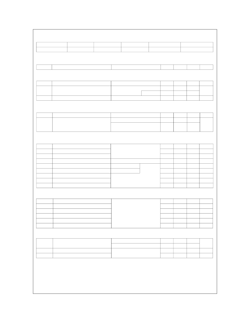
�Package� Marking� and� Ordering� Information�
�Device� Marking�
�FDB8443�
�Device�
�FDB8443�
�Package�
�TO-263AB�
�Reel� Size�
�330mm�
�Tape� Width�
�24mm�
�Quantity�
�800� units�
�Electrical� Characteristics� T� C� =� 25°C� unless� otherwise� noted�
�Symbol�
�Parameter�
�Test� Conditions�
�Min�
�Typ�
�Max�
�Unit�
�Off� Characteristics�
�B� VDSS�
�Drain� to� Source� Breakdown� Voltage�
�I� D� =� 250� μ� A,� V� GS� =� 0V�
�40�
�-�
�-�
�V�
�I� DSS�
�I� GSS�
�Zero� Gate� Voltage� Drain� Current�
�Gate� to� Source� Leakage� Current�
�V� DS� =� 32V,�
�V� GS� =� 0V�
�V� GS� =� ±20V�
�T� C� =� 150� o� C�
�-�
�-�
�-�
�-�
�-�
�-�
�1�
�250�
�±100�
�μ� A�
�nA�
�On� Characteristics�
�V� GS(th)�
�r� DS(on)�
�Gate� to� Source� Threshold� Voltage�
�Drain� to� Source� On� Resistance�
�V� GS� =� V� DS� ,� I� D� =� 250� μ� A�
�I� D� =� 80A,� V� GS� =� 10V�
�I� D� =� 80A,� V� GS� =� 10V,�
�T� J� =� 175� o� C�
�2�
�-�
�-�
�2.8�
�2.3�
�4.2�
�4�
�3.0�
�5.5�
�V�
�m� Ω�
�Dynamic� Characteristics�
�C� iss�
�C� oss�
�C� rss�
�R� G�
�Q� g(TOT)�
�Input� Capacitance�
�Output� Capacitance�
�Reverse� Transfer� Capacitance�
�Gate� Resistance�
�Total� Gate� Charge� at� 10V�
�V� DS� =� 25V,� V� GS� =� 0V,�
�f� =� 1MHz�
�V� GS� =� 0.5V,� f� =� 1MHz�
�V� GS� =� 0� to� 10V�
�-�
�-�
�-�
�-�
�-�
�9310�
�800�
�510�
�0.9�
�142�
�-�
�-�
�-�
�-�
�185�
�pF�
�pF�
�pF�
�Ω�
�nC�
�Q� g(TH)�
�Q� gs�
�Q� gs2�
�Q� gd�
�Threshold� Gate� Charge�
�Gate� to� Source� Gate� Charge�
�Gate� Charge� Threshold� to� Plateau�
�Gate� to� Drain� “Miller“� Charge�
�V� GS� =� 0� to� 2V�
�V� DD� =� 20V�
�I� D� =� 35A�
�I� g� =� 1mA�
�-�
�-�
�-�
�-�
�17.5�
�36�
�18.8�
�32�
�23�
�-�
�-�
�-�
�nC�
�nC�
�nC�
�nC�
�Switching� Characteristics� (V� GS� =� 10V)�
�t� on�
�Turn-On� Time�
�-�
�-�
�58�
�ns�
�t� d(on)�
�t� r�
�t� d(off)�
�t� f�
�t� off�
�Turn-On� Delay� Time�
�Rise� Time�
�Turn-Off� Delay� Time�
�Fall� Time�
�Turn-Off� Time�
�V� DD� =� 20V,� I� D� =� 35A�
�V� GS� =� 10V,� R� GS� =� 2� Ω�
�-�
�-�
�-�
�-�
�-�
�18.4�
�17.9�
�55�
�13.5�
�-�
�-�
�-�
�-�
�-�
�109�
�ns�
�ns�
�ns�
�ns�
�ns�
�Drain-Source� Diode� Characteristics�
�V� SD�
�t� rr�
�Q� rr�
�Source� to� Drain� Diode� Voltage�
�Reverse� Recovery� Time�
�Reverse� Recovery� Charge�
�I� SD� =� 35A�
�I� SD� =� 15A�
�I� SD� =� 35A,� dI� SD� /dt� =� 100A/� μ� s�
�-�
�-�
�-�
�-�
�0.8�
�0.8�
�42�
�48�
�1.25�
�1.0�
�55�
�62�
�V�
�ns�
�nC�
�Notes:�
�1:� Starting� T� J� =� 25� o� C,� L� =� 0.26mH,� I� AS� =� 64A.�
�2:� Pulse� width� =� 100s.�
�?2010� Fairchild� Semiconductor� Corporation�
�FDB8443� Rev.� C1�
�2�
�www.fairchildsemi.com�
�相关PDF资料 |
PDF描述 |
|---|---|
| FDB8444 | MOSFET N-CH 40V 70A TO-263AB |
| FDB8445 | MOSFET N-CH 40V 70A D2PAK |
| FDB8447L | MOSFET N-CH 40V 15A D2PAK |
| FDB8453LZ | MOSFET N-CH 40V 16.1A TO-263AB |
| FDB86102LZ | MOSFET N-CH 100V 30A D2PAK |
相关代理商/技术参数 |
参数描述 |
|---|---|
| FDB8443_11 | 制造商:FAIRCHILD 制造商全称:Fairchild Semiconductor 功能描述:N-Channel PowerTrench?? MOSFET 40V, 80A, 3.0m?? |
| FDB8443_F085 | 功能描述:MOSFET 40V N-CHAN PwrTrench RoHS:否 制造商:STMicroelectronics 晶体管极性:N-Channel 汲极/源极击穿电压:650 V 闸/源击穿电压:25 V 漏极连续电流:130 A 电阻汲极/源极 RDS(导通):0.014 Ohms 配置:Single 最大工作温度: 安装风格:Through Hole 封装 / 箱体:Max247 封装:Tube |
| FDB8444 | 功能描述:MOSFET 40V N-Channel PowerTrench MOSFET RoHS:否 制造商:STMicroelectronics 晶体管极性:N-Channel 汲极/源极击穿电压:650 V 闸/源击穿电压:25 V 漏极连续电流:130 A 电阻汲极/源极 RDS(导通):0.014 Ohms 配置:Single 最大工作温度: 安装风格:Through Hole 封装 / 箱体:Max247 封装:Tube |
| FDB8444_10 | 制造商:FAIRCHILD 制造商全称:Fairchild Semiconductor 功能描述:N-Channel PowerTrench?? MOSFET 40V, 70A, 5.5m?? |
| FDB8444_F085 | 功能描述:MOSFET 40V N-Ch PowerTrench RoHS:否 制造商:STMicroelectronics 晶体管极性:N-Channel 汲极/源极击穿电压:650 V 闸/源击穿电压:25 V 漏极连续电流:130 A 电阻汲极/源极 RDS(导通):0.014 Ohms 配置:Single 最大工作温度: 安装风格:Through Hole 封装 / 箱体:Max247 封装:Tube |
发布紧急采购,3分钟左右您将得到回复。