- 您现在的位置:买卖IC网 > PDF目录67504 > FM3316-G SPECIALTY CONSUMER CIRCUIT, PDSO14 PDF资料下载
参数资料
| 型号: | FM3316-G |
| 元件分类: | 消费家电 |
| 英文描述: | SPECIALTY CONSUMER CIRCUIT, PDSO14 |
| 封装: | GREEN, MO-012AB, SOIC-14 |
| 文件页数: | 11/28页 |
| 文件大小: | 320K |
| 代理商: | FM3316-G |
第1页第2页第3页第4页第5页第6页第7页第8页第9页第10页当前第11页第12页第13页第14页第15页第16页第17页第18页第19页第20页第21页第22页第23页第24页第25页第26页第27页第28页
FM33256/FM3316 SPI Companion w/ FRAM
Rev. 2.0
Feb. 2009
Page 19 of 28
Command Structure
There are eight commands called op-codes that can
be issued by the bus master to the FM33xx. They are
listed in the table below. These op-codes control the
functions performed by the memory and Processor
Companion.
They
can
be
divided
into
three
categories. First, there are commands that have no
subsequent
operations.
They
perform
a
single
function, such as, enabling a write operation. Second
are commands followed by one data byte, either in or
out. They operate on the Status Register. The third
group includes commands for memory and Processor
Companion transactions followed by address and one
or more bytes of data.
Table 4. Op-code Commands
Name
Description
Op-code
WREN
Set Write Enable Latch
0000 0110b
WRDI
Write Disable
0000 0100b
RDSR
Read Status Register
0000 0101b
WRSR
Write Status Register
0000 0001b
READ
Read Memory Data
0000 0011b
WRITE
Write Memory Data
0000 0010b
RDPC
Read Proc. Companion
0001 0011b
WRPC
Write Proc. Companion
0001 0010b
WREN – Set Write Enable Latch
The FM33xx will power up with writes disabled. The
WREN command must be issued prior to any write
operation. Sending the WREN op-code will allow
the user to issue subsequent op-codes for write
operations.
These
include
writing
the
Status
Register, writing the Processor Companion, and
writing the memory.
Sending the WREN op-code causes the internal
Write Enable Latch to be set. A flag bit in the Status
Register, called WEL, indicates the state of the
latch. WEL=1 indicates that writes are permitted.
Attempting to write the WEL bit in the Status
Register has no effect on the state of this bit. The
WEL bit will automatically be cleared on the rising
edge of /CS following a WRDI, WRSR, WRPC, or
WRITE op-code. No other op-code affects the state
of the WEL bit. This prevents further writes to the
Status Register, F-RAM memory, or the companion
register space without another WREN command.
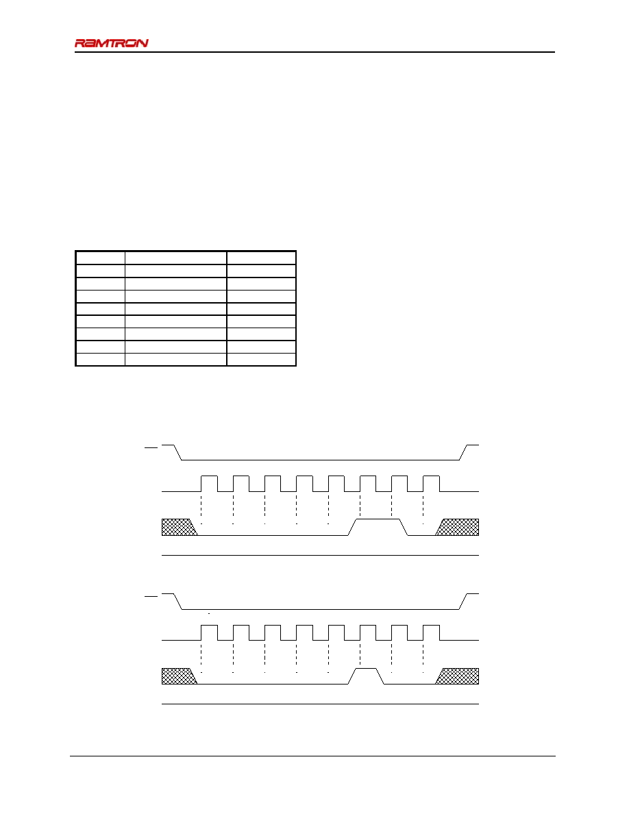
Figure 13 below illustrates the WREN command
bus configuration.
WRDI – Write Disable
The WRDI command disables all write activity by
clearing the Write Enable Latch. The user can verify
that writes are disabled by reading the WEL bit in
the Status Register and verifying that WEL=0.
Figure 14 illustrates the WRDI command bus
configuration.
Hi-Z
0
1
2
3
4
5
6
7
0
1
0
CS
SCK
SI
SO
Figure 13. WREN Bus Configuration
CS
SCK
SI
SO
Hi-Z
0
1
2
3
4
5
6
7
0
1
0
Figure 14. WRDI Bus Configuration
相关PDF资料 |
PDF描述 |
|---|---|
| FM33256-GTR | SPECIALTY CONSUMER CIRCUIT, PDSO14 |
| FM33256-G | SPECIALTY CONSUMER CIRCUIT, PDSO14 |
| FM4005-G | SPECIALTY CONSUMER CIRCUIT, PDSO14 |
| FME270-461/ES | 1 FUNCTIONS, 400 V, 1.5 A, DATA LINE FILTER |
| FME270-461V/ES | 1 FUNCTIONS, 400 V, 1.5 A, DATA LINE FILTER |
相关代理商/技术参数 |
参数描述 |
|---|---|
| FM3316-GTR | 功能描述:F-RAM 16K w/Pwr Mon WDT Bat Sw Pwr Fail RoHS:否 存储容量:512 Kbit 组织:64 K x 8 接口:SPI 工作电源电压:2 V to 3.6 V 工作温度范围:- 40 C to + 85 C 安装风格:SMD/SMT 封装 / 箱体:SOIC-8 封装:Tube 制造商:Cypress Semiconductor |
| FM33256 | 制造商:RAMTRON 制造商全称:RAMTRON 功能描述:3V Integrated Processor Companion with Memory |
| FM33256_09 | 制造商:RAMTRON 制造商全称:RAMTRON 功能描述:3V Integrated Processor Companion with Memory |
| FM33256B | 制造商:CYPRESS 制造商全称:Cypress Semiconductor 功能描述:3V Integrated Processor Companion with F-RAM |
| FM33256B-G | 功能描述:实时时钟 256Kb F-RAM Processor Companion RoHS:否 制造商:Microchip Technology 功能:Clock, Calendar. Alarm RTC 总线接口:I2C 日期格式:DW:DM:M:Y 时间格式:HH:MM:SS RTC 存储容量:64 B 电源电压-最大:5.5 V 电源电压-最小:1.8 V 最大工作温度:+ 85 C 最小工作温度: 安装风格:Through Hole 封装 / 箱体:PDIP-8 封装:Tube |
发布紧急采购,3分钟左右您将得到回复。