- 您现在的位置:买卖IC网 > PDF目录67504 > FM3316-G SPECIALTY CONSUMER CIRCUIT, PDSO14 PDF资料下载
参数资料
| 型号: | FM3316-G |
| 元件分类: | 消费家电 |
| 英文描述: | SPECIALTY CONSUMER CIRCUIT, PDSO14 |
| 封装: | GREEN, MO-012AB, SOIC-14 |
| 文件页数: | 17/28页 |
| 文件大小: | 320K |
| 代理商: | FM3316-G |
第1页第2页第3页第4页第5页第6页第7页第8页第9页第10页第11页第12页第13页第14页第15页第16页当前第17页第18页第19页第20页第21页第22页第23页第24页第25页第26页第27页第28页
FM33256/FM3316 SPI Companion w/ FRAM
Rev. 2.0
Feb. 2009
Page 24 of 28
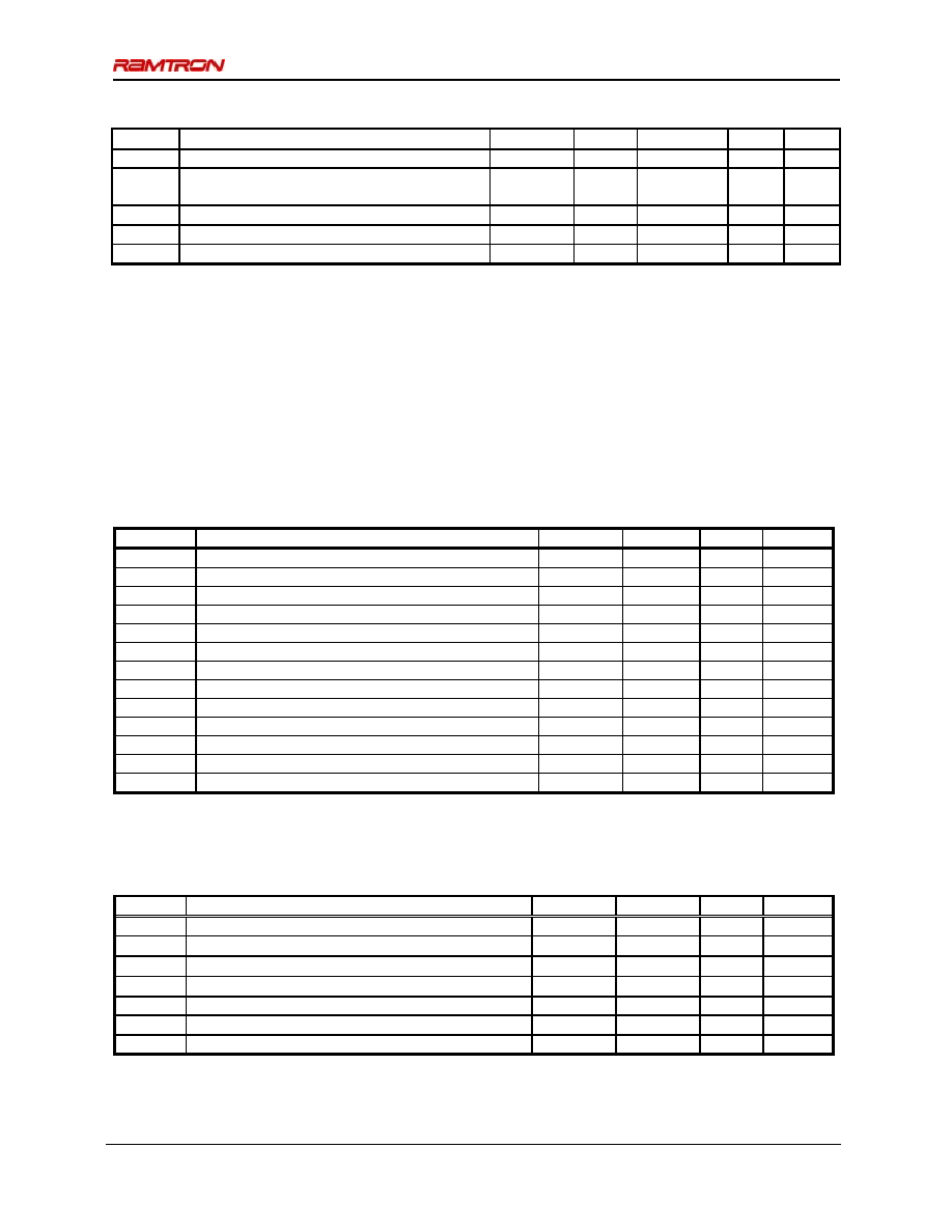
DC Operating Conditions, continued (TA = -40° C to + 85° C, VDD = 2.7V to 3.6V unless otherwise specified)
Symbol
Parameter
Min
Typ
Max
Units
Notes
VOL
Output Low Voltage @ IOL = 3 mA
-
0.4
V
VOH
Output High Voltage
(SO, PFO) @ IOH = -2 mA
VDD – 0.8
-
V
RRST
Pull-up resistance for /RST inactive
50
400
K
VPFI
Power Fail Input Reference Voltage
1.475
1.50
1.525
V
VHYS
Power Fail Input (PFI) Hysteresis (Rising)
-
100
mV
Notes
1.
Full complete operation. Supervisory circuits, RTC, etc operate to lower voltages as specified.
2.
SCK toggling between VDD-0.3V and VSS, other inputs VSS or VDD-0.3V.
3.
All inputs at VSS or VDD, static. Trickle charger off (VBC=0).
4.
The VBAK trickle charger automatically regulates the maximum voltage on this pin for capacitor backup applications.
5.
VBAK = 3.0V, VDD < VSW, oscillator running, CNT at VBAK.
6.
VBAK will source current when trickle charge is enabled (VBC bit=1), VDD > VBAK, and VBAK < VBAK max.
7.
This is the VDD supply current contributed by enabling the trickle charger circuit, and does not account for IBAKTC.
8.
This is the VDD supply current contributed by enabling the watchdog circuit, WDE=1 and WDET set to a non-zero value.
9.
/RST is asserted active when VDD < VTP .
10. The minimum VDD to guarantee the level of /RST remains a valid VOL level.
11. VIN or VOUT = VSS to VDD. Does not apply to PFI, X1, or X2.
12. Includes /RST input detection of external reset condition to trigger driving of /RST signal by FM33xx.
AC Parameters (TA = -40°C to + 85°C, VDD = 2.7V to 3.6V CL = 30 pF)
Symbol
Parameter
Min
Max
Units
Notes
fCK
SCK Clock Frequency
0
16
MHz
tCH
Clock High Time
28
ns
1
tCL
Clock Low Time
28
ns
1
tCSU
Chip Select Setup
10
ns
tCSH
Chip Select Hold
10
ns
tOD
Output Disable Time
20
ns
2
tODV
Output Data Valid Time
24
ns
tOH
Output Hold Time
0
ns
tD
Deselect Time
90
ns
tR
Data In Rise Time
50
ns
1,3
tF
Data In Fall Time
50
ns
1,3
tSU
Data Setup Time
6
ns
tH
Data Hold Time
6
ns
Notes
1.
tCH + tCL = 1/fCK.
2.
This parameter is characterized but not 100% tested.
3.
Rise and fall times measured between 10% and 90% of waveform.
Supervisor Timing (TA = -40° C to + 85° C, VDD = 2.7V to 3.6V)
Symbol
Parameter
Min
Max
Units
Notes
tRPW
/RST Pulse Width (active low time)
30
100
ms
tRNR
/RST Response Time to VDD<VTP (noise filter)
7
25
s
1
tVR
VDD Rise Time
50
-
s/V
1,2
tVF
VDD Fall Time
100
-
s/V
1,2
tWDST
Watchdog StartTime
0.3*tDOG1
tDOG1
ms
3
tWDET
Watchdog EndTime
tDOG2
3.3*tDOG2
ms
3
fCNT
Frequency of Event Counter
0
1
kHz
Notes
1
This parameter is characterized but not tested.
2
Slope measured at any point on VDD waveform.
相关PDF资料 |
PDF描述 |
|---|---|
| FM33256-GTR | SPECIALTY CONSUMER CIRCUIT, PDSO14 |
| FM33256-G | SPECIALTY CONSUMER CIRCUIT, PDSO14 |
| FM4005-G | SPECIALTY CONSUMER CIRCUIT, PDSO14 |
| FME270-461/ES | 1 FUNCTIONS, 400 V, 1.5 A, DATA LINE FILTER |
| FME270-461V/ES | 1 FUNCTIONS, 400 V, 1.5 A, DATA LINE FILTER |
相关代理商/技术参数 |
参数描述 |
|---|---|
| FM3316-GTR | 功能描述:F-RAM 16K w/Pwr Mon WDT Bat Sw Pwr Fail RoHS:否 存储容量:512 Kbit 组织:64 K x 8 接口:SPI 工作电源电压:2 V to 3.6 V 工作温度范围:- 40 C to + 85 C 安装风格:SMD/SMT 封装 / 箱体:SOIC-8 封装:Tube 制造商:Cypress Semiconductor |
| FM33256 | 制造商:RAMTRON 制造商全称:RAMTRON 功能描述:3V Integrated Processor Companion with Memory |
| FM33256_09 | 制造商:RAMTRON 制造商全称:RAMTRON 功能描述:3V Integrated Processor Companion with Memory |
| FM33256B | 制造商:CYPRESS 制造商全称:Cypress Semiconductor 功能描述:3V Integrated Processor Companion with F-RAM |
| FM33256B-G | 功能描述:实时时钟 256Kb F-RAM Processor Companion RoHS:否 制造商:Microchip Technology 功能:Clock, Calendar. Alarm RTC 总线接口:I2C 日期格式:DW:DM:M:Y 时间格式:HH:MM:SS RTC 存储容量:64 B 电源电压-最大:5.5 V 电源电压-最小:1.8 V 最大工作温度:+ 85 C 最小工作温度: 安装风格:Through Hole 封装 / 箱体:PDIP-8 封装:Tube |
发布紧急采购,3分钟左右您将得到回复。