- 您现在的位置:买卖IC网 > PDF目录67504 > FM33256-G SPECIALTY CONSUMER CIRCUIT, PDSO14 PDF资料下载
参数资料
| 型号: | FM33256-G |
| 元件分类: | 消费家电 |
| 英文描述: | SPECIALTY CONSUMER CIRCUIT, PDSO14 |
| 封装: | GREEN, MS-012AB, SOIC-14 |
| 文件页数: | 10/28页 |
| 文件大小: | 320K |
| 代理商: | FM33256-G |
第1页第2页第3页第4页第5页第6页第7页第8页第9页当前第10页第11页第12页第13页第14页第15页第16页第17页第18页第19页第20页第21页第22页第23页第24页第25页第26页第27页第28页
FM33256/FM3316 SPI Companion w/ FRAM
Rev. 2.0
Feb. 2009
Page 18 of 28
Serial Peripheral Interface – SPI Bus
The FM33xx employs a Serial Peripheral Interface
(SPI) bus. It is specified to operate at speeds up to
16 MHz. This high-speed serial bus provides high
performance
serial
communication
to
a
host
microcontroller.
Many common
microcontrollers
have hardware SPI ports allowing a direct interface.
It is quite simple to emulate the port using ordinary
port pins for microcontrollers that do not. The
FM33xx devices operate in SPI Mode 0 and 3.
The SPI interface uses a total of four pins: clock,
data-in, data-out, and chip select. A typical system
configuration uses an FM33xx and a standalone SPI
device with a microcontroller that has a dedicated
SPI port, as Figure 10 illustrates. Note that the clock,
data-in, and data-out pins are common among all
devices. The /CS pins must be driven separately for
the FM33xx and each additional SPI device.
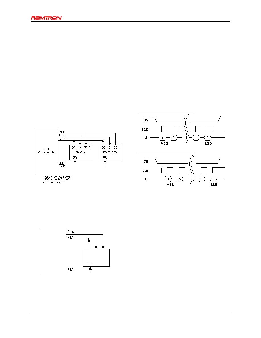
Figure 10. System Configuration with SPI port
For a microcontroller that has no dedicated SPI bus, a
general purpose port may be used. To reduce
hardware resources on the controller, it is possible to
connect the two data pins together. Figure 11 shows a
configuration that uses only three pins.
Microcontroller
FM33xx
SO
SI SCK
CS
Figure 11. System Configuration without SPI port
Protocol Overview
The SPI interface is a synchronous serial interface
using clock and data pins. It is intended to support
multiple devices on the bus. Each device is activated
using a chip select. Once chip select is activated by
the bus master, the FM33xx will begin monitoring
the clock and data lines. The relationship between
the falling edge of /CS, the clock and data is dictated
by the SPI mode. The device will make a
determination of the SPI mode on the falling edge of
each chip select. While there are four such modes,
the FM33xx supports only modes 0 and 3. Figure 12
shows the required signal relationships for modes 0
and 3.
For both modes, data is clocked into the
FM33xx on the rising edge of SCK and data is
expected on the first rising edge after /CS goes
active. If the clock starts from a high state, it will
fall prior to the first data transfer in order to create
the first rising edge.
SPI Mode 0: CPOL=0, CPHA=0
SPI Mode 3: CPOL=1, CPHA=1
Figure 12. SPI Modes 0 & 3
The SPI protocol is controlled by op-codes. These
op-codes specify the commands to the device. After
/CS is activated the first byte transferred from the
bus master is the op-code. Following the op-code,
any addresses and data are then transferred. Note
that the WREN and WRDI op-codes are commands
with no subsequent data transfer.
Important: The /CS pin must go inactive after an
operation is complete and before a new op-code
can be issued. There is only one valid op-code per
active chip select.
Data Transfer
All data transfers to and from the FM33xx occur in
8-bit groups. They are synchronized to the clock
signal (SCK), and they transfer most significant bit
(MSB) first.
Serial inputs are registered on the
rising edge of SCK. Outputs are driven from the
falling edge of SCK.
相关PDF资料 |
PDF描述 |
|---|---|
| FM4005-G | SPECIALTY CONSUMER CIRCUIT, PDSO14 |
| FME270-461/ES | 1 FUNCTIONS, 400 V, 1.5 A, DATA LINE FILTER |
| FME270-461V/ES | 1 FUNCTIONS, 400 V, 1.5 A, DATA LINE FILTER |
| FME270-461W/ES | 1 FUNCTIONS, 400 V, 1.5 A, DATA LINE FILTER |
| FME270-461Y/ES | 1 FUNCTIONS, 400 V, 1.5 A, DATA LINE FILTER |
相关代理商/技术参数 |
参数描述 |
|---|---|
| FM33256-GTR | 功能描述:F-RAM 256K w/Pwr Mon WDT Bat Sw Pwr Fail RoHS:否 存储容量:512 Kbit 组织:64 K x 8 接口:SPI 工作电源电压:2 V to 3.6 V 工作温度范围:- 40 C to + 85 C 安装风格:SMD/SMT 封装 / 箱体:SOIC-8 封装:Tube 制造商:Cypress Semiconductor |
| FM333 | 制造商:Black Box Corporation 功能描述:ST ADAPTER SNAP FITTING |
| FM334C | 制造商:Black Box Corporation 功能描述:GigaPlus Blank Wallplate Insert, Ivory, 20-Pack |
| FM335 | 制造商:Black Box Corporation 功能描述:BLANK SNAP FITTING 10 PAK ELECTRICAL IVORY |
| FM336 | 制造商:Black Box Corporation 功能描述:GigaStation Blank Snap Fitting, Gray, 10-Pack |
发布紧急采购,3分钟左右您将得到回复。