- 您现在的位置:买卖IC网 > PDF目录10624 > FMS6690MTC20X (Fairchild Semiconductor)IC VIDEO FILTER DRVR 6CH 20TSSOP PDF资料下载
参数资料
| 型号: | FMS6690MTC20X |
| 厂商: | Fairchild Semiconductor |
| 文件页数: | 10/11页 |
| 文件大小: | 0K |
| 描述: | IC VIDEO FILTER DRVR 6CH 20TSSOP |
| 标准包装: | 1 |
| 类型: | 视频滤波器 |
| 应用: | 录音机,机顶盒 |
| 安装类型: | 表面贴装 |
| 封装/外壳: | 20-TSSOP(0.173",4.40mm 宽) |
| 供应商设备封装: | 20-TSSOP |
| 包装: | 标准包装 |
| 产品目录页面: | 1214 (CN2011-ZH PDF) |
| 其它名称: | FMS6690MTC20XDKR |
2006 Fairchild Semiconductor Corporation
www.fairchildsemi.com
FMS6690 Rev. 1.0.3
8
FM
S6690
—
Six
C
h
annel,
6
th
Order,
SD/PS/HD
Video
Filt
er
Driver
Applications Information
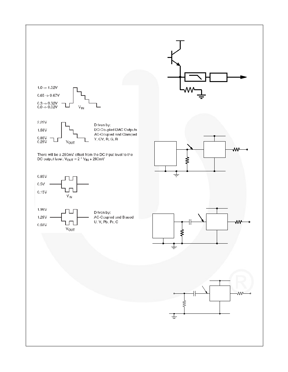
Functional Description
The FMS6690 Low-Cost Video Filter (LCVF) provides
6dB gain (9dB optional, contact factory for further
information) from input to output. In addition, the input is
slightly offset to optimize the output driver performance.
The offset is held to the minimum required value to
decrease the standing DC current into the load. Typical
voltage levels are shown in Figure 14.
Figure 14. Typical Voltage Levels
The FMS6690 provides an internal diode clamp to
support AC-coupled input signals. If the input signal
does not go below ground, the input clamp does not
operate. This allows DAC outputs to directly drive the
FMS6690 without an AC coupling capacitor. The worst-
case sync tip compression, due to the clamp, does not
exceed 7mV. The input level set by the clamp,
combined with the internal DC offset, keeps the output
within acceptable range. When the input is AC-coupled,
the diode clamp sets the sync tip (or lowest voltage) just
below ground.
For symmetric signals like C, U, V, Cb, Cr, Pb, and Pr;
the average DC bias is fairly constant and the inputs
can be AC-coupled with the addition of a pull-up resistor
to set the DC input voltage. DAC outputs can also drive
these same signals without the AC coupling capacitor.
A conceptual illustration of the input clamp circuit is
shown in Figure 15.
YOUT
800k
Driver
YIN
0.65V
Figure 15. Input Clamp Circuit
I/O Configurations
For DC-coupled DAC drive with DC-coupled outputs,
use the configuration in Figure 16.
DVD or
STB
SoC
DAC
Output
75
Ω
LCVF
Clamp
Inactive
0V- 1.4V
Figure 16. DC-Coupled Inputs and Outputs
Alternatively, if the DAC’s average DC output level
causes the signal to exceed the range of 0V to 1.4V, it
can be AC-coupled, as shown in Figure 17.
DVD or
STB
SoC
DAC
Output
75
Ω
LCVF
Clamp
Active
0.1
0V- 1.4V
Figure 17. AC-Coupled Inputs, DC-coupled Outputs
When the FMS6690 is driven by an unknown external
source or a SCART with its own clamping circuitry, the
inputs should be AC-coupled, shown in Figure 18.
75
Ω
LCVF
Clamp
Active
75
Ω
0.1
External Video
source must
be AC-coupled.
0V- 1.4V
Figure 18. SCART with DC-Coupled Outputs
相关PDF资料 |
PDF描述 |
|---|---|
| VE-BWM-IV-F4 | CONVERTER MOD DC/DC 10V 150W |
| FMS6346MTC20X | IC DRIVER VIDEO FLTR 6CH 20TSSOP |
| VE-BWM-IV-F3 | CONVERTER MOD DC/DC 10V 150W |
| MAX3223ECAP+ | IC TXRX RS232 250KBPS SD 20SSOP |
| VE-BWM-IV-F1 | CONVERTER MOD DC/DC 10V 150W |
相关代理商/技术参数 |
参数描述 |
|---|---|
| FMS6G10US60 | 功能描述:IGBT 模块 600V 10A MODULE RoHS:否 制造商:Infineon Technologies 产品:IGBT Silicon Modules 配置:Dual 集电极—发射极最大电压 VCEO:600 V 集电极—射极饱和电压:1.95 V 在25 C的连续集电极电流:230 A 栅极—射极漏泄电流:400 nA 功率耗散:445 W 最大工作温度:+ 125 C 封装 / 箱体:34MM 封装: |
| FMS6G10US60S | 功能描述:IGBT 模块 600V 10A MODULE RoHS:否 制造商:Infineon Technologies 产品:IGBT Silicon Modules 配置:Dual 集电极—发射极最大电压 VCEO:600 V 集电极—射极饱和电压:1.95 V 在25 C的连续集电极电流:230 A 栅极—射极漏泄电流:400 nA 功率耗散:445 W 最大工作温度:+ 125 C 封装 / 箱体:34MM 封装: |
| FMS6G15US60 | 功能描述:IGBT 模块 600V 15A MODULE RoHS:否 制造商:Infineon Technologies 产品:IGBT Silicon Modules 配置:Dual 集电极—发射极最大电压 VCEO:600 V 集电极—射极饱和电压:1.95 V 在25 C的连续集电极电流:230 A 栅极—射极漏泄电流:400 nA 功率耗散:445 W 最大工作温度:+ 125 C 封装 / 箱体:34MM 封装: |
| FMS6G15US60S | 功能描述:IGBT 模块 600V 15A MODULE RoHS:否 制造商:Infineon Technologies 产品:IGBT Silicon Modules 配置:Dual 集电极—发射极最大电压 VCEO:600 V 集电极—射极饱和电压:1.95 V 在25 C的连续集电极电流:230 A 栅极—射极漏泄电流:400 nA 功率耗散:445 W 最大工作温度:+ 125 C 封装 / 箱体:34MM 封装: |
| FMS6G20US60 | 功能描述:IGBT 模块 IGBT Module RoHS:否 制造商:Infineon Technologies 产品:IGBT Silicon Modules 配置:Dual 集电极—发射极最大电压 VCEO:600 V 集电极—射极饱和电压:1.95 V 在25 C的连续集电极电流:230 A 栅极—射极漏泄电流:400 nA 功率耗散:445 W 最大工作温度:+ 125 C 封装 / 箱体:34MM 封装: |
发布紧急采购,3分钟左右您将得到回复。