- 您现在的位置:买卖IC网 > PDF目录9177 > FS6377-01G-XTD (ON Semiconductor)IC CLOCK GEN 3-PLL PROGR 16-SOIC PDF资料下载
参数资料
| 型号: | FS6377-01G-XTD |
| 厂商: | ON Semiconductor |
| 文件页数: | 18/24页 |
| 文件大小: | 0K |
| 描述: | IC CLOCK GEN 3-PLL PROGR 16-SOIC |
| 标准包装: | 48 |
| 类型: | PLL 时钟发生器 |
| PLL: | 是 |
| 输入: | 晶体 |
| 输出: | CMOS |
| 电路数: | 1 |
| 比率 - 输入:输出: | 1:4 |
| 差分 - 输入:输出: | 无/无 |
| 频率 - 最大: | 230MHz |
| 除法器/乘法器: | 是/无 |
| 电源电压: | 3 V ~ 5.5 V |
| 工作温度: | 0°C ~ 70°C |
| 安装类型: | 表面贴装 |
| 封装/外壳: | 16-SOIC(0.154",3.90mm 宽) |
| 供应商设备封装: | 16-SOIC |
| 包装: | 管件 |
| 产品目录页面: | 1115 (CN2011-ZH PDF) |
| 其它名称: | 766-1026 |
FS6377
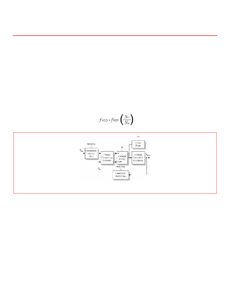
3.0 Functional Block Description
3.1 Phase Locked Loops (PLLs)
Each of the three on-chip PLLs is a standard phase- and frequency-locked loop architecture that multiplies a reference frequency to a
desired frequency by a ratio of integers. This frequency multiplication is exact.
As shown in Figure 3, each PLL consists of a reference divider, a phase-frequency detector (PFD), a charge pump, an internal loop
filter, a voltage-controlled oscillator (VCO), and a feedback divider.
During operation, the reference frequency (fREF), generated by the on-board crystal oscillator, is first reduced by the reference divider.
The divider value is called the "modulus," and is denoted as NR for the reference divider. The divided reference is then fed into the PFD.
The PFD controls the frequency of the VCO (fVCO) through the charge pump and loop filter. The VCO provides a high speed, low noise,
continuously variable frequency clock source for the PLL. The output of the VCO is fed back to the PFD through the feedback divider
(the modulus is denoted by NF) to close the loop.
The PFD will drive the VCO up or down in frequency until the divided reference frequency and the divided VCO frequency appearing at
the inputs of the PFD are equal. The input/output relationship between the reference frequency and the VCO frequency is:
Figure 3: PLL Diagram
3.1.1. Reference Divider
The reference divider is designed for low phase jitter. The divider accepts the output of the reference oscillator and provides a divided-
down frequency to the PFD. The reference divider is an 8-bit divider, and can be programmed for any modulus from 1 to 255 by
programming the equivalent binary value. A divide-by-256 can also be achieved by programming the eight bits to 00h.
3.1.2. Feedback Divider
The feedback divider is based on a dual-modulus prescaler technique. The technique allows the same granularity as a fully
programmable feedback divider, while still allowing the programmable portion to operate at low speed. A high-speed pre-divider (also
called a prescaler) is placed between the VCO and the programmable feedback divider because of the high speeds at which the VCO
can operate. The dual-modulus technique insures reliable operation at any speed that the VCO can achieve and reduces the overall
power consumption of the divider.
Rev. 4 | Page 3 of 24 | www.onsemi.com
相关PDF资料 |
PDF描述 |
|---|---|
| VE-BW3-MY-F4 | CONVERTER MOD DC/DC 24V 50W |
| MC12093DR2G | IC PRESCALER 2/4/8 1.1GHZ 8-SOIC |
| VI-B72-MW-B1 | CONVERTER MOD DC/DC 15V 100W |
| DS1866+ | IC POT TRIM LOG 2.7-5.5V 8-DIP |
| VI-B6V-MW-B1 | CONVERTER MOD DC/DC 5.8V 100W |
相关代理商/技术参数 |
参数描述 |
|---|---|
| FS6377-01G-XTP | 功能描述:时钟发生器及支持产品 I2C PROG 3-PLL CLK RoHS:否 制造商:Silicon Labs 类型:Clock Generators 最大输入频率:14.318 MHz 最大输出频率:166 MHz 输出端数量:16 占空比 - 最大:55 % 工作电源电压:3.3 V 工作电源电流:1 mA 最大工作温度:+ 85 C 安装风格:SMD/SMT 封装 / 箱体:QFN-56 |
| FS6377-01IG-XTD | 功能描述:时钟发生器及支持产品 I2C PROG 3-PLL CLK (IND) RoHS:否 制造商:Silicon Labs 类型:Clock Generators 最大输入频率:14.318 MHz 最大输出频率:166 MHz 输出端数量:16 占空比 - 最大:55 % 工作电源电压:3.3 V 工作电源电流:1 mA 最大工作温度:+ 85 C 安装风格:SMD/SMT 封装 / 箱体:QFN-56 |
| FS6377-01IG-XTP | 功能描述:时钟发生器及支持产品 I2C PROG 3-PLL CLK IND RoHS:否 制造商:Silicon Labs 类型:Clock Generators 最大输入频率:14.318 MHz 最大输出频率:166 MHz 输出端数量:16 占空比 - 最大:55 % 工作电源电压:3.3 V 工作电源电流:1 mA 最大工作温度:+ 85 C 安装风格:SMD/SMT 封装 / 箱体:QFN-56 |
| FS-662 | 功能描述:模块化系统 - SOM A9M2440 Module 32MB 10Mbps Ethernet RoHS:否 制造商:Digi International 外观尺寸:ConnectCore 9P 处理器类型:ARM926EJ-S 频率:150 MHz 存储容量:8 MB, 16 MB 存储类型:NOR Flash, SDRAM 接口类型:I2C, SPI, UART 工作电源电压:3.3 V 最大工作温度:+ 85 C 尺寸:1.97 in x 1.97 in x 6.1 in |
| FS6713-20-07 | 制造商:Schaffner 功能描述: |
发布紧急采购,3分钟左右您将得到回复。