- 您现在的位置:买卖IC网 > PDF目录383019 > GS81032A (GSI TECHNOLOGY) 1Mb(32K x 32Bit)Synchronous Burst SRAM(1M位(32K x 32位)同步静态RAM(带2位脉冲地址计数器)) PDF资料下载
参数资料
| 型号: | GS81032A |
| 厂商: | GSI TECHNOLOGY |
| 英文描述: | 1Mb(32K x 32Bit)Synchronous Burst SRAM(1M位(32K x 32位)同步静态RAM(带2位脉冲地址计数器)) |
| 中文描述: | 1兆(32KX8的32位)同步突发静态存储器(100万位(32K的× 32位)同步静态随机存储器(带2位脉冲地址计数器)) |
| 文件页数: | 9/23页 |
| 文件大小: | 756K |
| 代理商: | GS81032A |
Rev: 1.00 12/2000
Specifications cited are subject to change without notice. For latest documentation see http://www.gsitechnology.com.
9/23
2000, Giga Semiconductor, Inc.
GS81032AT/Q-150/138/133/117/100/66
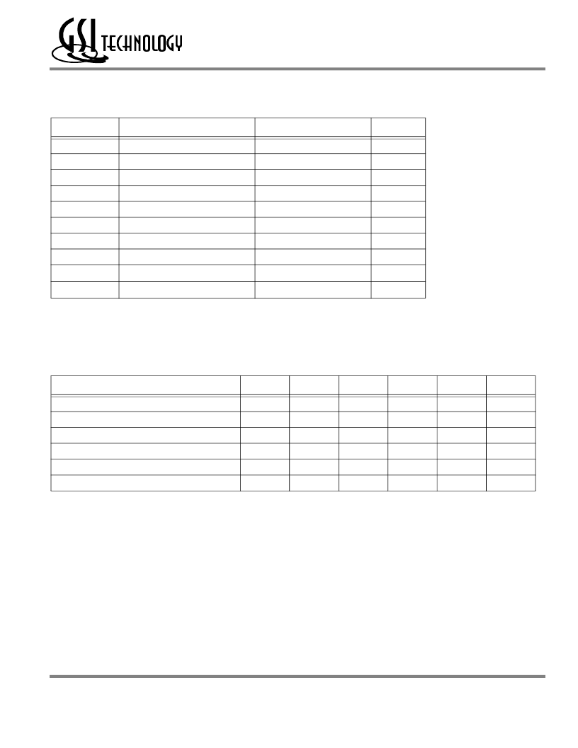
Absolute Maximum Ratings
(All voltages reference to V
SS
)
Note:
Permanent damage to the device may occur if the Absolute Maximum Ratings are exceeded. Operation should be restricted to Recommended
Operating Conditions. Exposure to conditions exceeding the Absolute Maximum Ratings, for an extended period of time, may affect reliability of
this component.
Recommended Operating Conditions
Notes:
1.
Unless otherwise noted, all performance specifications quoted are evaluated for worst case at both 2.75 V
≤
V
DDQ
≤
2.375 V (i.e., 2.5 V I/O)
and 3.6 V
≤
V
DDQ
≤
3.135 V (i.e., 3.3 V I/O) and quoted at whichever condition is worst case.
This device features input buffers compatible with both 3.3 V and 2.5 V I/O drivers.
Most speed grades and configurations of this device are offered in both Commercial and Industrial Temperature ranges. The part number of
Industrial Temperature Range versions end the character “I”. Unless otherwise noted, all performance specifications quoted are evaluated
for worst case in the temperature range marked on the device.
Input Under/overshoot voltage must be –2 V > Vi < V
DD
+2 V with a pulse width not to exceed 20% tKC.
2.
3.
4.
Symbol
Description
Value
Unit
V
DD
V
DDQ
V
CK
V
I/O
V
IN
I
IN
I
OUT
P
D
T
STG
T
BIAS
Voltage on V
DD
Pins
Voltage in V
DDQ
Pins
Voltage on Clock Input Pin
–0.5 to 4.6
V
–0.5 to V
DD
-0.5 to 6
V
V
Voltage on I/O Pins
–0.5 to V
DDQ
+0.5 (
≤
4.6 V max.)
–0.5 to V
DD
+0.5 (
≤
4.6 V max.)
+/–20
V
Voltage on Other Input Pins
V
Input Current on Any Pin
mA
Output Current on Any I/O Pin
+/–20
mA
Package Power Dissipation
1.5
W
Storage Temperature
–55 to 125
o
C
Temperature Under Bias
–55 to 125
o
C
Parameter
Symbol
Min.
Typ.
Max.
Unit
Notes
Supply Voltage
V
DD
V
DDQ
V
IH
V
IL
T
A
T
A
3.135
3.3
3.6
V
DD
V
—
I/O Supply Voltage
2.375
2.5
V
1
Input High Voltage
1.7
—
V
DD
+0.3
0.8
V
2
Input Low Voltage
–0.3
—
V
°
C
°
C
2
Ambient Temperature (Commercial Range Versions)
0
25
70
3
Ambient Temperature (Industrial Range Versions)
–40
25
85
3
相关PDF资料 |
PDF描述 |
|---|---|
| GS815018 | 16Mb(1M x 18Bit)Synchronous Burst SRAM(16M位(1M x 18位)同步静态RAM(带2位脉冲地址计数器)) |
| GS815032 | 16Mb(512K x 32Bit)Synchronous Burst SRAM(16M位(512K x 32位)同步静态RAM(带2位脉冲地址计数器)) |
| GS815036 | 16Mb(512K x 36Bit)Synchronous Burst SRAM(16M位(512K x 36位)同步静态RAM(带2位脉冲地址计数器)) |
| GS8150E18 | 16Mb(1M x 18Bit)Synchronous Burst SRAM(16M位(1M x 18位)同步静态RAM(带2位脉冲地址计数器)) |
| GS8150E32 | 16Mb(512K x 32Bit)Synchronous Burst SRAM(16M位(512K x 32位)同步静态RAM(带2位脉冲地址计数器)) |
相关代理商/技术参数 |
参数描述 |
|---|---|
| GS81032A2T-138 | 制造商:GSI 制造商全称:GSI Technology 功能描述:32K x 32 1M Synchronous Burst SRAM |
| GS81032AQ-133 | 制造商:GSI 制造商全称:GSI Technology 功能描述:32K x 32 1M Synchronous Burst SRAM |
| GS81032AQ-133I | 制造商:GSI 制造商全称:GSI Technology 功能描述:32K x 32 1M Synchronous Burst SRAM |
| GS81032AQ-138 | 制造商:GSI 制造商全称:GSI Technology 功能描述:32K x 32 1M Synchronous Burst SRAM |
| GS81032AQ-138I | 制造商:GSI 制造商全称:GSI Technology 功能描述:32K x 32 1M Synchronous Burst SRAM |
发布紧急采购,3分钟左右您将得到回复。