- 您现在的位置:买卖IC网 > PDF目录60615 > GSC24BC16 (GTM CORPORATION) 2-WIRE SERIAL EEPROMS PDF资料下载
参数资料
| 型号: | GSC24BC16 |
| 厂商: | GTM CORPORATION |
| 英文描述: | 2-WIRE SERIAL EEPROMS |
| 中文描述: | 2线串行EEPROM |
| 文件页数: | 4/9页 |
| 文件大小: | 305K |
| 代理商: | GSC24BC16 |
GSC24BC01/02/02/04/08/16
Page: 4/9
ISSUED DATE :2006/06/14
REVISED DATE :
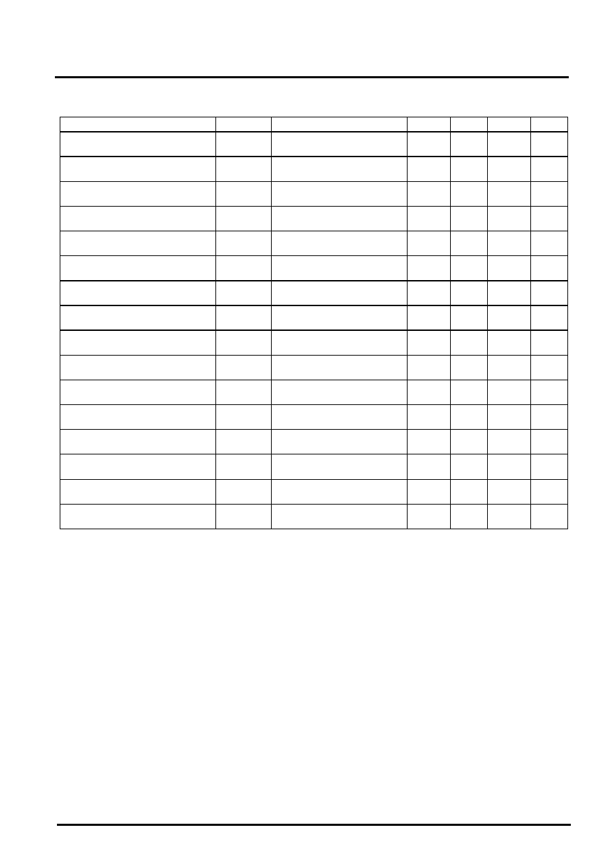
AC Characteristics Applicable over recommended operating range from: TA=-40 ~ +85 : ,
VCC=+1.8 ~ 5.5V, CL=1 TTL Gate & 100pF (unless otherwise noted)
Parameter
Symbol
Test Condition
Min
TYP
Max
Unit
Clock Frequency, SCL
fSCL
VCC=1.8V
VCC=2.7 ~ 5.5V
-
100
400
KHz
Clock Pulse Width Low
tLOW
VCC=1.8V
VCC=2.7 ~ 5.5V
4.7
1.2
-
s
Clock Pulse Width High
tHIGH
VCC=1.8V
VCC=2.7 ~ 5.5V
4.0
0.6
-
s
Noise Suppression Time (1)
tI
VCC=1.8V
VCC=2.7 ~ 5.5V
-
100
50
ns
Clock Low to Data Out Valid
tAA
VCC=1.8V
VCC=2.7 ~ 5.5V
0.1
-
4.5
0.9
s
Time the bus must be free before
a new transmission can start (1)
tBUF
VCC=1.8V
VCC=2.7 ~ 5.5V
4.7
1.2
-
s
Start Hold Time
tHD.STA
VCC=1.8V
VCC=2.7 ~ 5.5V
4.0
0.6
-
s
Start Setup Time
tSU.STA
VCC=1.8V
VCC=2.7 ~ 5.5V
4.7
0.6
-
s
Data in Hold Time
tHD.DAT V
CC
=1.8V
VCC=2.7 ~ 5.5V
0
-
s
Data in Setup Time
tUS.DAT
VCC=1.8V
VCC=2.7 ~ 5.5V
200
100
-
ns
Input Rise Time (1)
tR
VCC=1.8V
VCC=2.7 ~ 5.5V
-
1.0
0.3
s
Input Fall Time (1)
tF
VCC=1.8V
VCC=2.7 ~ 5.5V
-
300
ns
Stop Setup Time
tSU.STO V
CC
=1.8V
VCC=2.7 ~ 5.5V
4.7
0.6
-
s
Data Out Hold Time
tDH
VCC=1.8V
VCC=2.7 ~ 5.5V
100
50
-
ns
Write Cycle Time
tWR
VCC=1.8V
VCC=2.7 ~ 5.5V
-
5
ms
5.0V, 25 : , Byte Mode
Endurance
(1)
VCC=1.8V
VCC=2.7 ~ 5.5V
1M
-
Write
Cycles
Note: 1. This parameter is characterized and not 100% tested.
Device Operation
Clock and Data Transitions: Transitions on the SDA pin should only occur when SCL is low (refer to the Data
Validity timing diagram in Figure 5). If the SDA pin changes when SCL is high, then the transition will be
interpreted as a START or STOP condition.
START Condition: A START condition occurs when the SDA transitions form high to low when SCL is high.
The START signal is usually used to initiate a command (refer to the Start and Stop Definition timing diagram in
Figure 6).
STOP Condition: A STOP condition occurs when the SDA transitions form low to high when SCL is high (refer
to Figure 6. START and STOP Definition timing diagram). The STOP command will put the device into standby
mode after no acknowledgment is issued during the read sequence.
Acknowledge: An acknowledgement is sent by pulling the SDA low to confirm that a word has been
successfully received. All addresses and data words are serially transmitted to and from the EEPROM in 8-bit
words, so acknowledgments are usually issued during the 9th clock cycle.
Standby Mode: Standby mode is entered when the chip is initially powered-on or after a STOP command has
been issued and any internal operations have been completed. .
Memory Reset: In the event of unexpected power or connection loss, a START condition can be issued to
restart the input command sequence. If the device is currently in write cycle mode, this command will be
ignored.
相关PDF资料 |
PDF描述 |
|---|---|
| GSC2596M | 150 KHz, 2A PWM Step-Down DC/DC Converter |
| GSC3842 | HIGH PERFORMANCE CURRENT MODE CONTROLERS |
| GSC3843 | HIGH PERFORMANCE CURRENT MODE CONTROLERS |
| GSC4081 | NPN EPITAXIAL PLANAR TRANSISTOR |
| GSC4404 | N-CHANNEL ENHANCEMENT MODE POWER MOSFET |
相关代理商/技术参数 |
参数描述 |
|---|---|
| GSC-24D/B | 制造商:Crydom 功能描述: |
| GSC25 | 制造商:SLPOWER 制造商全称:SL Power Electronics 功能描述:25 Watt Global Performance Switchers |
| GSC2596M | 制造商:GTM 制造商全称:GTM 功能描述:150 KHz, 2A PWM Step-Down DC/DC Converter |
| GSC25A | 功能描述:线性和开关式电源 25W +5.1/+12/-12V RoHS:否 制造商:TDK-Lambda 产品:Switching Supplies 开放式框架/封闭式:Enclosed 输出功率额定值:800 W 输入电压:85 VAC to 265 VAC 输出端数量:1 输出电压(通道 1):20 V 输出电流(通道 1):40 A 商用/医用: 输出电压(通道 2): 输出电流(通道 2): 安装风格:Rack 长度: 宽度: 高度: |
| GSC25AG | 功能描述:线性和开关式电源 25W +5.1/+12/-12V RoHS:否 制造商:TDK-Lambda 产品:Switching Supplies 开放式框架/封闭式:Enclosed 输出功率额定值:800 W 输入电压:85 VAC to 265 VAC 输出端数量:1 输出电压(通道 1):20 V 输出电流(通道 1):40 A 商用/医用: 输出电压(通道 2): 输出电流(通道 2): 安装风格:Rack 长度: 宽度: 高度: |
发布紧急采购,3分钟左右您将得到回复。