参数资料
| 型号: | HFA1112IB |
| 厂商: | Intersil |
| 文件页数: | 9/14页 |
| 文件大小: | 0K |
| 描述: | IC BUFFER 850MHZ 8-SOIC |
| 标准包装: | 98 |
| 放大器类型: | 缓冲器 |
| 电路数: | 1 |
| 转换速率: | 2400 V/µs |
| -3db带宽: | 850MHz |
| 电流 - 输入偏压: | 25µA |
| 电压 - 输入偏移: | 8000µV |
| 电流 - 电源: | 21mA |
| 电流 - 输出 / 通道: | 60mA |
| 电压 - 电源,单路/双路(±): | 9 V ~ 11 V,±4.5 V ~ 5.5 V |
| 工作温度: | -40°C ~ 85°C |
| 安装类型: | 表面贴装 |
| 封装/外壳: | 8-SOIC(0.154",3.90mm 宽) |
| 供应商设备封装: | 8-SOIC |
| 包装: | 管件 |
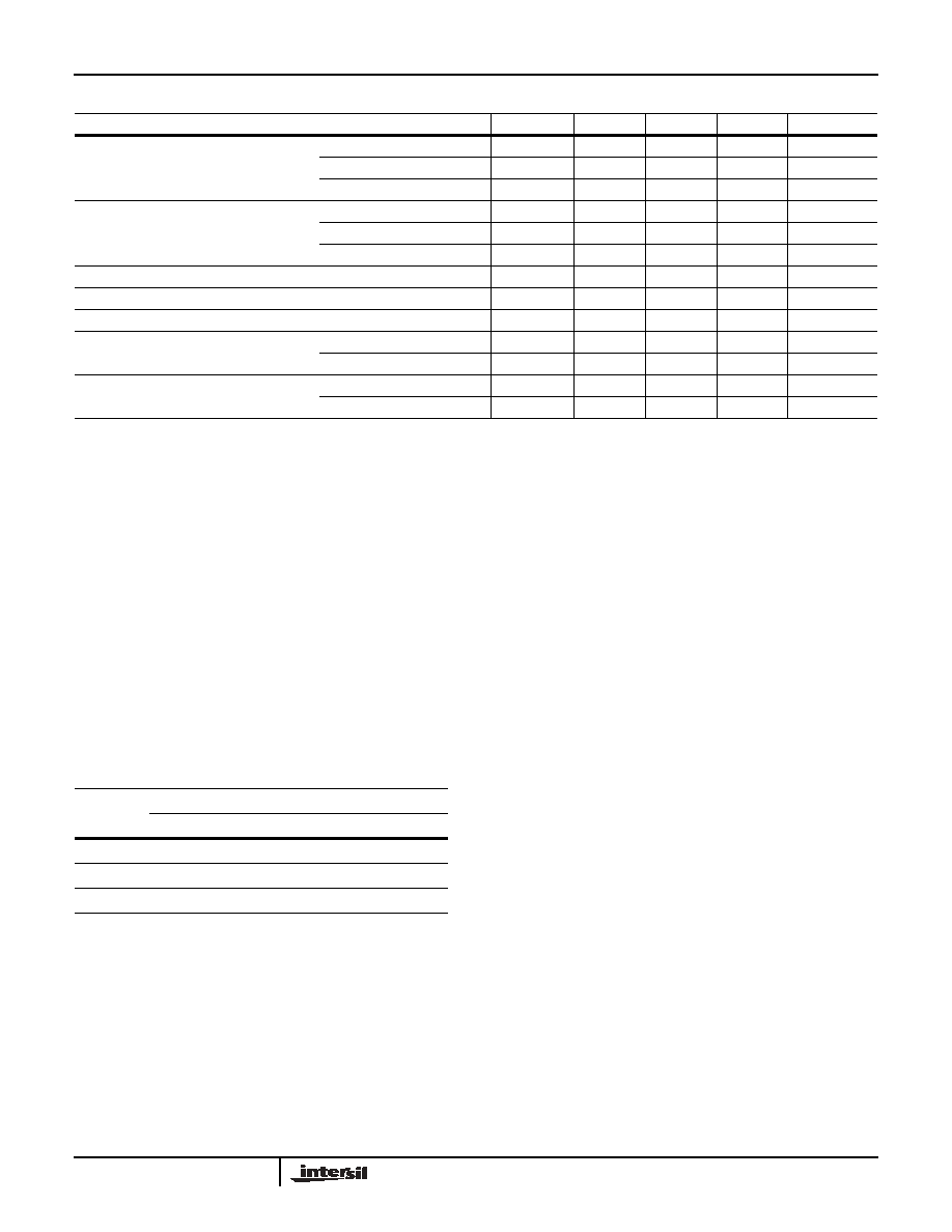
4
Application Information
Closed Loop Gain Selection
The HFA1112 features a novel design which allows the user
to select from three closed loop gains, without any external
components. The result is a more flexible product, fewer part
types in inventory, and more efficient use of board space.
This “buffer” operates in closed loop gains of -1, +1, or +2, and
gain selection is accomplished via connections to the
±inputs.
Applying the input signal to +IN and floating -IN selects a gain
of +1, while grounding -IN selects a gain of +2. A gain of -1 is
obtained by applying the input signal to -IN with +IN grounded.
The table below summarizes these connections:
PC Board Layout
The frequency response of this amplifier depends greatly on
the amount of care taken in designing the PC board. The
use of low inductance components such as chip
resistors and chip capacitors is strongly recommended,
while a solid ground plane is a must!
Attention should be given to decoupling the power supplies.
A large value (10
F) tantalum in parallel with a small value
(0.1
F) chip capacitor works well in most cases.
Terminated microstrip signal lines are recommended at the
input and output of the device. Capacitance directly on the
output must be minimized, or isolated as discussed in the
next section.
For unity gain applications, care must also be taken to
minimize the capacitance to ground seen by the amplifier’s
inverting input. At higher frequencies this capacitance will
tend to short the -INPUT to GND, resulting in a closed loop
gain which increases with frequency. This will cause
excessive high frequency peaking and potentially other
problems as well.
An example of a good high frequency layout is the
Evaluation Board shown in Figure 2.
Driving Capacitive Loads
Capacitive loads, such as an A/D input, or an improperly
terminated transmission line will degrade the amplifier’s
phase margin resulting in frequency response peaking and
possible oscillations. In most cases, the oscillation can be
avoided by placing a resistor (RS) in series with the output
prior to the capacitance.
Figure 1 details starting points for the selection of this
resistor. The points on the curve indicate the RS and CL
combinations for the optimum bandwidth, stability, and
settling time, but experimental fine tuning is recommended.
Picking a point above or to the right of the curve yields an
overdamped response, while points below or left of the curve
indicate areas of underdamped performance.
RS and CL form a low pass network at the output, thus
limiting system bandwidth well below the amplifier
bandwidth of 850MHz. By decreasing RS as CLincreases
Rise Time
(VOUT = 2V Step)
AV = -1
25
-
0.82
-
ns
AV = +1
25
-
1.06
-
ns
AV = +2
25
-
1.00
-
ns
Overshoot
(VOUT = 0.5V Step, Input tR/tF = 200ps,
Notes 2, 3, 4)
AV = -1
25
-
12
30
%
AV = +1
25
-
45
65
%
AV = +2
25
-
6
20
%
0.1% Settling Time (Note 3)
VOUT = 2V to 0V
25
-
11
-
ns
0.05% Settling Time
VOUT = 2V to 0V
25
-
15
-
ns
Overdrive Recovery Time
VIN = 5VP-P
25
-
8.5
-
ns
Differential Gain
AV = +1, 3.58MHz, RL = 150
25
-
0.03
-
%
AV = +2, 3.58MHz, RL = 150
25
-
0.02
-
%
Differential Phase
AV = +1, 3.58MHz, RL = 150
25
-
0.05
-
Degrees
AV = +2, 3.58MHz, RL = 150
25
-
0.04
-
Degrees
NOTES:
2. This parameter is not tested. The limits are guaranteed based on lab characterization, and reflect lot-to-lot variation.
3. See Typical Performance Curves for more information.
4. Overshoot decreases as input transition times increase, especially for AV = +1. Please refer to Typical Performance Curves.
Electrical Specifications VSUPPLY = ±5V, AV = +1, RL = 100, Unless Otherwise Specified (Continued)
PARAMETER
TEST CONDITIONS
TEMP (oC)
MIN
TYP
MAX
UNITS
GAIN
(ACL)
CONNECTIONS
+INPUT (PIN 3)
-INPUT (PIN 2)
-1
GND
Input
+1
Input
NC (Floating)
+2
Input
GND
HFA1112
相关PDF资料 |
PDF描述 |
|---|---|
| 8-1879208-1 | RES 22.0K OHM 1/16W 0.1% 0402 |
| AS168X-CB1H030 | CIRCUIT BRKR THERMAL 3.0A 1POLE |
| AD8572AR-REEL | IC OPAMP CHOPPER R-R DUAL 8SOIC |
| 8-1879213-5 | RES 226 OHM 1/16W 0.1% 0402 |
| MCP6001RT-I/OT | IC OPAMP SGL 1.8V R-R SOT23-5 |
相关代理商/技术参数 |
参数描述 |
|---|---|
| HFA1112IB96 | 功能描述:IC BUFFER 850MHZ 8-SOIC RoHS:否 类别:集成电路 (IC) >> Linear - Amplifiers - Instrumentation 系列:- 标准包装:50 系列:LinCMOS™ 放大器类型:通用 电路数:4 输出类型:- 转换速率:0.05 V/µs 增益带宽积:110kHz -3db带宽:- 电流 - 输入偏压:0.7pA 电压 - 输入偏移:210µV 电流 - 电源:57µA 电流 - 输出 / 通道:30mA 电压 - 电源,单路/双路(±):3 V ~ 16 V,±1.5 V ~ 8 V 工作温度:-40°C ~ 85°C 安装类型:表面贴装 封装/外壳:14-SOIC(0.154",3.90mm 宽) 供应商设备封装:14-SOIC 包装:管件 产品目录页面:865 (CN2011-ZH PDF) 其它名称:296-1834296-1834-5 |
| HFA1112IBZ | 功能描述:运算放大器 - 运放 W/ANNEAL BUFFER 850M HZCFBPRG-GAN8SOICIND RoHS:否 制造商:STMicroelectronics 通道数量:4 共模抑制比(最小值):63 dB 输入补偿电压:1 mV 输入偏流(最大值):10 pA 工作电源电压:2.7 V to 5.5 V 安装风格:SMD/SMT 封装 / 箱体:QFN-16 转换速度:0.89 V/us 关闭:No 输出电流:55 mA 最大工作温度:+ 125 C 封装:Reel |
| HFA1112IBZ96 | 功能描述:运算放大器 - 运放 W/ANNEAL BUFR 850MHZ CFB PRG-GAIN IND RoHS:否 制造商:STMicroelectronics 通道数量:4 共模抑制比(最小值):63 dB 输入补偿电压:1 mV 输入偏流(最大值):10 pA 工作电源电压:2.7 V to 5.5 V 安装风格:SMD/SMT 封装 / 箱体:QFN-16 转换速度:0.89 V/us 关闭:No 输出电流:55 mA 最大工作温度:+ 125 C 封装:Reel |
| HFA1112IJ | 制造商:Rochester Electronics LLC 功能描述:- Bulk |
| HFA1112IP | 功能描述:IC AMP BUFFER 850MHZ 8-PDIP RoHS:否 类别:集成电路 (IC) >> Linear - Amplifiers - Instrumentation 系列:- 标准包装:50 系列:- 放大器类型:通用 电路数:2 输出类型:满摆幅 转换速率:1.8 V/µs 增益带宽积:6.5MHz -3db带宽:4.5MHz 电流 - 输入偏压:5nA 电压 - 输入偏移:100µV 电流 - 电源:65µA 电流 - 输出 / 通道:35mA 电压 - 电源,单路/双路(±):1.8 V ~ 5.25 V,±0.9 V ~ 2.625 V 工作温度:-40°C ~ 85°C 安装类型:表面贴装 封装/外壳:10-TFSOP,10-MSOP(0.118",3.00mm 宽) 供应商设备封装:10-MSOP 包装:管件 |
发布紧急采购,3分钟左右您将得到回复。