参数资料
| 型号: | HFA1113IBZ |
| 厂商: | Intersil |
| 文件页数: | 12/16页 |
| 文件大小: | 0K |
| 描述: | IC BUFFER 850MHZ 8-SOIC |
| 标准包装: | 98 |
| 放大器类型: | 缓冲器 |
| 电路数: | 1 |
| 转换速率: | 2400 V/µs |
| -3db带宽: | 850MHz |
| 电流 - 输入偏压: | 25µA |
| 电压 - 输入偏移: | 8000µV |
| 电流 - 电源: | 21mA |
| 电流 - 输出 / 通道: | 60mA |
| 电压 - 电源,单路/双路(±): | 9 V ~ 11 V,±4.5 V ~ 5.5 V |
| 工作温度: | -40°C ~ 85°C |
| 安装类型: | 表面贴装 |
| 封装/外壳: | 8-SOIC(0.154",3.90mm 宽) |
| 供应商设备封装: | 8-SOIC |
| 包装: | 管件 |
5
FN1342.6
July 11, 2005
Application Information
Closed Loop Gain Selection
The HFA1113 features a novel design which allows the user
to select from three closed loop gains, without any external
components. The result is a more flexible product, fewer part
types in inventory, and more efficient use of board space.
This “buffer” operates in closed loop gains of -1, +1, or +2,
and gain selection is accomplished via connections to the
±Inputs. Applying the input signal to +IN and floating -IN
selects a gain of +1, while grounding -IN selects a gain of
+2. A gain of -1 is obtained by applying the input signal to
-IN with +IN grounded.
The table below summarizes these connections:
PC Board Layout
The frequency response of this amplifier depends greatly on
the amount of care taken in designing the PC board. The
use of low inductance components such as chip
resistors and chip capacitors is strongly recommended,
while a solid ground plane is a must!
Attention should be given to decoupling the power supplies.
A large value (10
F) tantalum in parallel with a small value
chip (0.1
F) capacitor works well in most cases.
Terminated microstrip signal lines are recommended at the
input and output of the device. Capacitance directly on the
output must be minimized, or isolated as discussed in the
next section.
For unity gain applications, care must also be taken to
minimize the capacitance to ground seen by the amplifier’s
inverting input. At higher frequencies this capacitance will
tend to short the -INPUT to GND, resulting in a closed loop
gain which increases with frequency. This will cause
excessive high frequency peaking and potentially other
problems as well.
An example of a good high frequency layout is the
Evaluation Board shown in Figure 3.
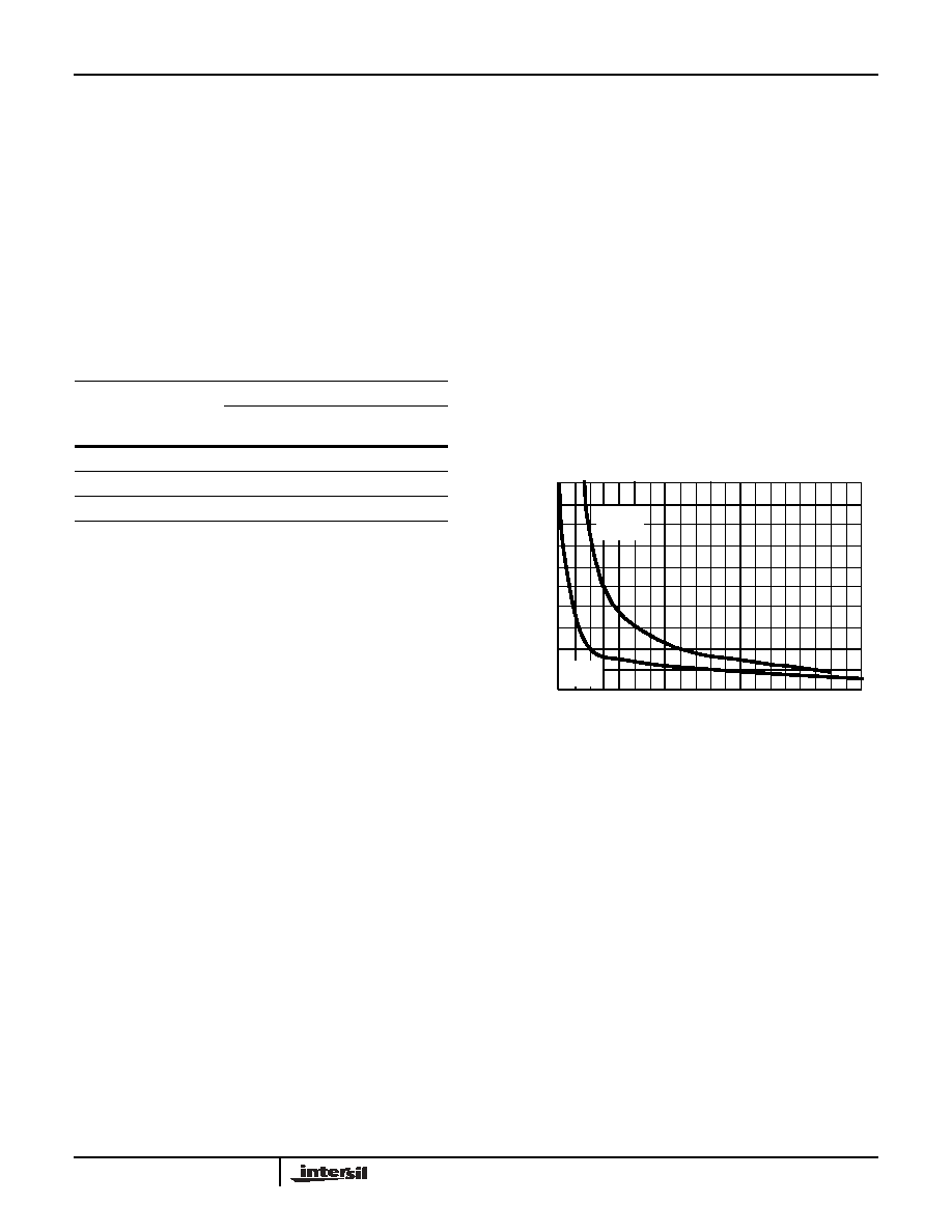
Driving Capacitive Loads
Capacitive loads, such as an A/D input, or an improperly
terminated transmission line will degrade the amplifier’s
phase margin resulting in frequency response peaking and
possible oscillations. In most cases, the oscillation can be
avoided by placing a resistor (RS) in series with the output
prior to the capacitance.
Figure 1 details starting points for the selection of this
resistor. The points on the curve indicate the RS and CL
combinations for the optimum bandwidth, stability, and
settling time, but experimental fine tuning is recommended.
Picking a point above or to the right of the curve yields an
overdamped response, while points below or left of the curve
indicate areas of underdamped performance.
RS and CL form a low pass network at the output, thus
limiting system bandwidth well below the amplifier bandwidth
of 850MHz. By decreasing RS as CLincreases (as illustrated
in the curves), the maximum bandwidth is obtained without
sacrificing stability. Even so, bandwidth does decrease as
you move to the right along the curve. For example, at
AV =+1, RS = 50, CL = 30pF, the overall bandwidth is
limited to 300MHz, and bandwidth drops to 100MHz at
AV =+1, RS = 5, CL = 340pF.
Evaluation Board
The performance of the HFA1113 may be evaluated using
the HFA11XX Evaluation Board, slightly modified as follows:
1. Remove the 500
feedback resistor (R2), and leave the
connection open.
2. a. For AV = +1 evaluation, remove the 500 gain setting
resistor (R1), and leave pin 2 floating.
b. For AV = +2, replace the 500 gain setting resistor with
a 0
resistor to GND.
The modified schematic and layout of the board are shown in
Figures 2 and 3.
To order evaluation boards (part number HFA11XXEVAL),
please contact your local sales office.
NOTE: The SOIC version may be evaluated in the DIP board by
using a SOIC-to-DIP adapter such as Aries Electronics Part Number
08-350000-10.
GAIN (ACL)
CONNECTIONS
+INPUT
(PIN 3)
-INPUT
(PIN 2)
-1
GND
Input
+1
Input
NC (Floating)
+2
Input
GND
R
S
(
)
LOAD CAPACITANCE (pF)
50
45
40
35
30
25
20
15
10
5
0
40
80
120
160
200
240
280
320
360
400
AV = +1
AV = +2
FIGURE 1. RECOMMENDED SERIES RESISTOR vs LOAD
CAPACITANCE
HFA1113
相关PDF资料 |
PDF描述 |
|---|---|
| HFA1130IBZ | IC OP AMP 850MHZ CFB 8-SOIC |
| HFA1412IP | IC BUFFER QUAD 350MHZ LP 14-DIP |
| HS18 | HEATSINK 12P PDIP |
| HSP-3 | THERMAL PAD TRIPLE PHASE |
| HSP-5 | THERMAL PAD 3-PHASE W/ADHESIVE |
相关代理商/技术参数 |
参数描述 |
|---|---|
| HFA1113IBZ96 | 功能描述:运算放大器 - 运放 W/ANNEAL BUFR 850MHZ CFB PRG-GAIN CLMP RoHS:否 制造商:STMicroelectronics 通道数量:4 共模抑制比(最小值):63 dB 输入补偿电压:1 mV 输入偏流(最大值):10 pA 工作电源电压:2.7 V to 5.5 V 安装风格:SMD/SMT 封装 / 箱体:QFN-16 转换速度:0.89 V/us 关闭:No 输出电流:55 mA 最大工作温度:+ 125 C 封装:Reel |
| HFA1113IP | 制造商:Rochester Electronics LLC 功能描述:- Bulk |
| HFA1113MJ/883 | 制造商:Rochester Electronics LLC 功能描述:- Bulk |
| HFA1113ML/883 | 制造商:Intersil Corporation 功能描述:SP AMP BFFR AMP SGL 20CLCC - Rail/Tube |
| HFA1114 | 制造商:INTERSIL 制造商全称:Intersil Corporation 功能描述:850MHz Video Cable Driving Buffer |
发布紧急采购,3分钟左右您将得到回复。