- 您现在的位置:买卖IC网 > PDF目录385376 > HFA3860BIV96 (HARRIS SEMICONDUCTOR) nullDirect Sequence Spread Spectrum Baseband Processor PDF资料下载
参数资料
| 型号: | HFA3860BIV96 |
| 厂商: | HARRIS SEMICONDUCTOR |
| 元件分类: | 无绳电话/电话 |
| 英文描述: | nullDirect Sequence Spread Spectrum Baseband Processor |
| 中文描述: | TELECOM, CELLULAR, BASEBAND CIRCUIT, PQFP48 |
| 文件页数: | 5/40页 |
| 文件大小: | 272K |
| 代理商: | HFA3860BIV96 |
第1页第2页第3页第4页当前第5页第6页第7页第8页第9页第10页第11页第12页第13页第14页第15页第16页第17页第18页第19页第20页第21页第22页第23页第24页第25页第26页第27页第28页第29页第30页第31页第32页第33页第34页第35页第36页第37页第38页第39页第40页
4-5
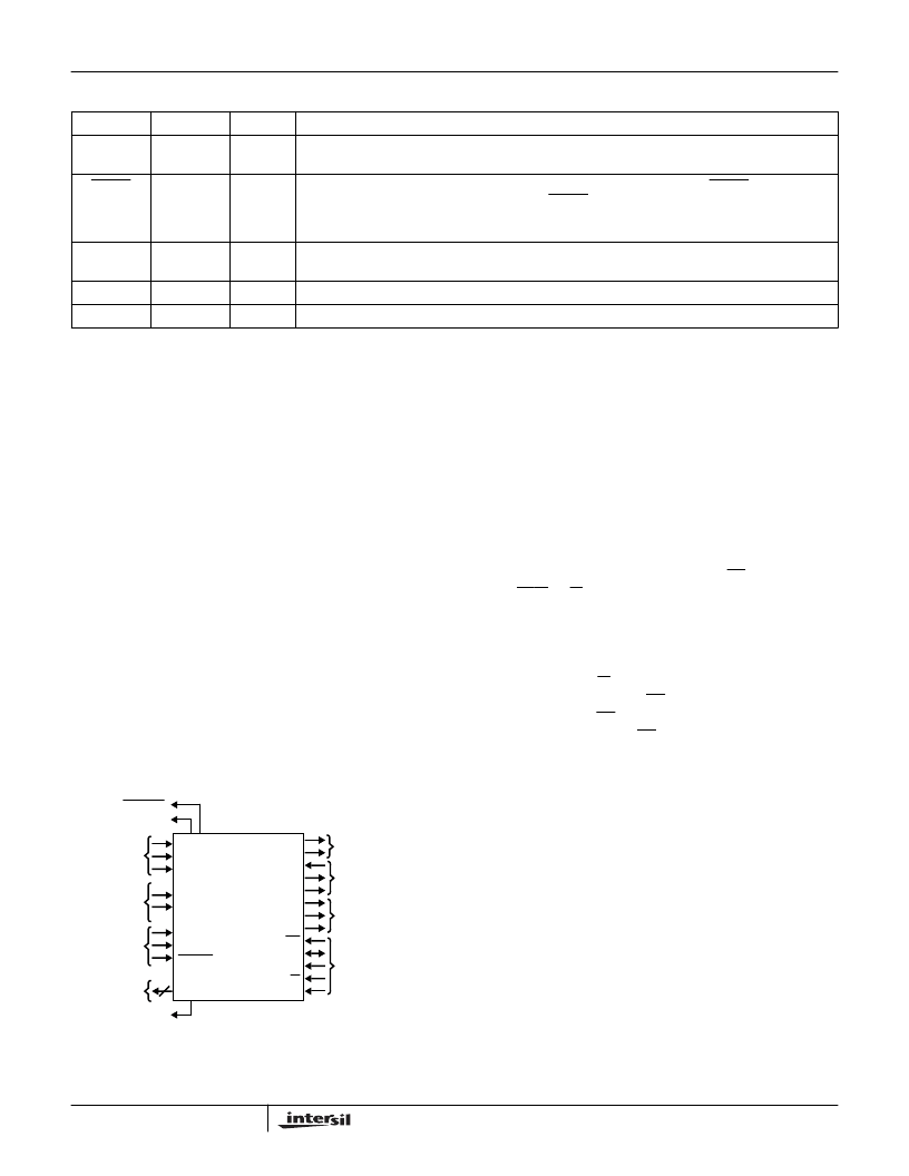
External Interfaces
There are three primary digital interface ports for the
HFA3860B that are used for configuration and during normal
operation of the device as shown in Figure 1. These ports are:
The
Control Port
, which is used to configure, write
and/or read the status of the internal HFA3860B
registers.
The
TX Port
, which is used to accept the data that
needs to be transmitted from the network processor.
The
RX Port
, which is used to output the received
demodulated data to the network processor.
In addition to these primary digital interfaces the device
includes a byte wide parallel
Test Port
which can be
configured to output various internal signals and/or data.
The device can also be set into various power consumption
modes by external control. The HFA3860B contains three
Analog to Digital (A/D) converters. The analog interfaces to
the HFA3860B include, the In phase (I) and Quadrature (Q)
data component inputs, and the RF signal strength indicator
input. A reference voltage divider is also required external to
the device.
Control Port (4 Wire)
The serial control port is used to serially write and read data
to/from the device. This serial port can operate up to a
11MHz rate or 1/2 the maximum master clock rate of the
device, MCLK (whichever is lower). MCLK must be running
during programming. This port is used to program and to
read all internal registers. The first 8 bits always represent
the address followed immediately by the 8 data bits for that
register. The two LSBs of address are don’t care, but
reserved for future expansion. The serial transfers are
accomplished through the serial data pin (SD). SD is a
bidirectional serial data bus. Chip Select (CS), and
Read/Write (R/W) are also required as handshake signals
for this port. The clock used in conjunction with the address
and data on SD is SCLK. This clock is provided by the
external source and it is an input to the HFA3860B. The
timing relationships of these signals are illustrated in
Figures 2 and 3. R/W is high when data is to be read, and
low when it is to be written. CS is an asynchronous reset to
the state machine. CS must be active (low) during the
entire data transfer cycle. CS selects the serial control port
device only. The serial control port operates
asynchronously from the TX and RX ports and it can
accomplish data transfers independent of the activity at the
other digital or analog ports.
The HFA3860B has 34 internal registers that can be
configured through the control port. These registers are
listed in the Configuration and Control Internal Register
table. Table 1 lists the configuration register number, a brief
name describing the register, and the HEX address to
access each of the registers. The type indicates whether the
corresponding register is Read only (R) or Read/Write
(R/W). Some registers are two bytes wide as indicated on
the table (high and low bytes). To fully program the
HFA3860B registers requires two writes of registers CR16
and CR17. This shadow register scheme extends the
register compliment by two registers from 32 to 34 without
requiring an additional address bit.
TEST_CK
1
O
This is the clock that is used in conjunction with the data that is being output from the test bus (TEST
0-7).
RESET
28
I
Master reset for device. When active TX and RX functions are disabled. If RESET is kept low the
HFA3860B goes into the power standby mode. RESET does not alter any of the configuration register
values nor does it preset any of the registers into default values. Device requires programming upon
power-up.
MCLK
30
I
Master Clock for device. The nominal frequency of this clock is 44MHz. This is used internally to
generate all other internal necessary clocks and is divided by 2 or 4 for the transceiver clocks.
I
OUT
48
O
TX Spread baseband I digital output data. Data is output at the chip rate.
Q
OUT
47
O
TX Spread baseband Q digital output data. Data is output at the chip rate.
NOTE: Total of 48 pins; ALL pins are used.
Pin Descriptions
(Continued)
NAME
PIN
TYPE I/O
DESCRIPTION
TXD
TXCLK
TX_RDY
RXD
RXCLK
MD_RDY
CS
SD
SCLK
R/W
SDI
I (ANALOG)
Q (ANALOG)
RSSI (ANALOG)
V
REFN
V
REFP
TX_PE
RX_PE
RESET
TEST
TX_PORT
RX_PORT
CONTROL_PORT
ANALOG
INPUTS
A/D
REFERENCE
POWER
DOWN
SIGNALS
TEST
PORT
9
HFA3860B
FIGURE 1. EXTERNAL INTERFACE
ANTSEL
ANTSEL
TESTCK
TX OUTPUTS
Q
I
HFA3860B
相关PDF资料 |
PDF描述 |
|---|---|
| HFA3861BIN | Direct Sequence Spread Spectrum Baseband Processor |
| HFA3861BIN96 | Direct Sequence Spread Spectrum Baseband Processor |
| HFA3925IA | null2.4GHz - 2.5GHz 250mW Power Amplifier |
| HFA3925IA96 | null2.4GHz - 2.5GHz 250mW Power Amplifier |
| HFA50PA60C | RxxP2xx Series - Econoline Unregulated DC-DC Converters; Input Voltage (Vdc): 05V; Output Voltage (Vdc): 15V; Power: 2W; EN 60950 certified, rated for 250VAC; UL-60950-1 / CSA C22.2 certified; 5.2kVDC Isolation for 1 Minute; Optional Continuous Short Circuit Protected; Wide Operating Temperature Range atfull 2 Watts Load, ?40??C to +85??C; Twin Chamber Transformer System; UL94V-0 Package Material; Efficiency to 80% |
相关代理商/技术参数 |
参数描述 |
|---|---|
| HFA3860IV | 制造商:Rochester Electronics LLC 功能描述:- Bulk 制造商:Harris Corporation 功能描述: |
| HFA3860IV WAF | 制造商:Harris Corporation 功能描述: |
| HFA3860IV96 | 制造商:INTERSIL 制造商全称:Intersil Corporation 功能描述:11 Mbps Direct Sequence Spread Spectrum Baseband Processor |
| HFA3861 | 制造商:INTERSIL 制造商全称:Intersil Corporation 功能描述:Direct Sequence Spread Spectrum Baseband Processor |
| HFA3861A | 制造商:INTERSIL 制造商全称:Intersil Corporation 功能描述:Direct Sequence Spread Spectrum Baseband Processo |
发布紧急采购,3分钟左右您将得到回复。