- 您现在的位置:买卖IC网 > PDF目录385376 > HFA3861BIN96 (INTERSIL CORP) Direct Sequence Spread Spectrum Baseband Processor PDF资料下载
参数资料
| 型号: | HFA3861BIN96 |
| 厂商: | INTERSIL CORP |
| 元件分类: | 无绳电话/电话 |
| 英文描述: | Direct Sequence Spread Spectrum Baseband Processor |
| 中文描述: | TELECOM, CELLULAR, BASEBAND CIRCUIT, PQFP64 |
| 封装: | 10 X 10 MM, PLASTIC, MS-026ACD, TQFP-64 |
| 文件页数: | 4/36页 |
| 文件大小: | 733K |
| 代理商: | HFA3861BIN96 |
第1页第2页第3页当前第4页第5页第6页第7页第8页第9页第10页第11页第12页第13页第14页第15页第16页第17页第18页第19页第20页第21页第22页第23页第24页第25页第26页第27页第28页第29页第30页第31页第32页第33页第34页第35页第36页
4
External Interfaces
There are three primary digital interface ports for the
HFA3861B that are used for configuration and during
normal operation of the device as shown in Figure 1. These
ports are:
The
read the status of the internal HFA3861B registers.
Control Port
, which is used to configure, write and/or
The
to be transmitted from the network processor.
TX Port
, which is used to accept the data that needs
The
demodulated data to the network processor.
RX Port
, which is used to output the received
In addition to these primary digital interfaces the device
includes a byte wide parallel
Test Port
which can be
configured to output various internal signals and/or data. The
device can also be set into various power consumption
modes by external control. The HFA3861B contains three
Analog to Digital (A/D) converters and four Digital to Analog
converters. The analog interfaces to the HFA3861B include,
the In phase (I) and quadrature (Q) data component inputs/
outputs, and the RF and IF receive automatic gain control
and transmit output power control.
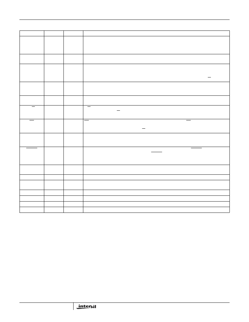
MD_RDY
54
O
MD_RDY is an output signal to the network processor, indicating header data and a data packet are
ready to be transferred to the processor. MD_RDY is an active high signal that signals the start of data
transfer over the RXD serial bus. MD_RDY goes active when the SFD (Note) is detected and returns
to its inactive state when RX_PE goes inactive or an error is detected in the header.
RX_PE
61
I
When active, the receiver is configured to be operational, otherwise the receiver is in standby mode.
This is an active high input signal. In standby, RX_PE inactive, all RX A/D converters are disabled.
SD
3
I/O
SD is a serial bidirectional data bus which is used to transfer address and data to/from the internal
registers. The bit ordering of an 8-bit word is MSB first. The first 8 bits during transfers indicate the
register address immediately followed by 8 more bits representing the data that needs to be written or
read at that register. In the 4 wire interface mode, this pin is three-stated unless the R/W pin is high.
SCLK
4
I
SCLK is the clock for the SD serial bus. The data on SD is clocked at the rising edge. SCLK is an input
clock and it is asynchronous to the internal master clock (MCLK). The maximum rate of this clock is
11MHz or one half the master clock frequency, whichever is lower.
SDI
64
I
Serial Data Input in 3 wire mode described in Tech Brief 383. This pin is not used in the 4 wire interface
described in this data sheet. It should not be left floating.
R/W
5
I
R/W is an input to the HFA3861B used to change the direction of the SD bus when reading or writing
data on the SD bus. R/W must be set up prior to the rising edge of SCLK. A high level indicates read
while a low level is a write.
CS
6
I
CS is a Chip select for the device to activate the serial control port. The CS doesn’t impact any of the
other interface ports and signals, i.e., the TX or RX ports and interface signals. This is an active low
signal. When inactive SD, SCLK, and R/W become “don’t care” signals.
TEST 7:0
51, 50, 49,
48, 47, 46,
45, 44
I/O
This is a data port that can be programmed to bring out internal signals or data for monitoring. These
bits are primarily reserved by the manufacturer for testing. A further description of the test port is given
in the appropriate section of this data sheet.
RESET
63
I
Master reset for device. When active TX and RX functions are disabled. If RESET is kept low the
HFA3861B goes into the power standby mode. RESET does not alter any of the configuration register
values nor does it preset any of the registers into default values. Device requires programming upon
power-up See the section on Control Register 12 bit 7 for important initialization information.
MCLK
42
I
Master Clock for device. The nominal frequency of this clock is 44MHz. This is used internally to
generate all other internal necessary clocks and is divided by 2 or 4 for the transceiver clocks.
TXI
+/-
23/24
O
TX Spread baseband I digital output data. Data is output at the chip rate. Balanced differential 23+/24-.
TXQ
+/-
29/30
O
TX Spread baseband Q digital output data. Data is output at the chip rate. Balanced differential
29+/30-.
CompCap
33
I
Compensation Capacitor.
CompCap2
26
I
Compensation Capacitor.
CompRes1
32
I
Compensation Resistor.
CompRes2
27
I
Compensation Resistor.
NOTE: See CR10[3].
Pin Descriptions
(Continued)
NAME
PIN
TYPE I/O
DESCRIPTION
HFA3861B
相关PDF资料 |
PDF描述 |
|---|---|
| HFA3925IA | null2.4GHz - 2.5GHz 250mW Power Amplifier |
| HFA3925IA96 | null2.4GHz - 2.5GHz 250mW Power Amplifier |
| HFA50PA60C | RxxP2xx Series - Econoline Unregulated DC-DC Converters; Input Voltage (Vdc): 05V; Output Voltage (Vdc): 15V; Power: 2W; EN 60950 certified, rated for 250VAC; UL-60950-1 / CSA C22.2 certified; 5.2kVDC Isolation for 1 Minute; Optional Continuous Short Circuit Protected; Wide Operating Temperature Range atfull 2 Watts Load, ?40??C to +85??C; Twin Chamber Transformer System; UL94V-0 Package Material; Efficiency to 80% |
| HFB50PA60C | Ultrafast, Soft Recovery Diode |
| HFA5250 | 500MHz, Ultra High Speed Monolithic Pin Driver |
相关代理商/技术参数 |
参数描述 |
|---|---|
| HFA3861IV | 制造商:INTERSIL 制造商全称:Intersil Corporation 功能描述:Direct Sequence Spread Spectrum Baseband Processor |
| HFA3861IV96 | 制造商:INTERSIL 制造商全称:Intersil Corporation 功能描述:Direct Sequence Spread Spectrum Baseband Processor |
| HFA3863 | 制造商:INTERSIL 制造商全称:Intersil Corporation 功能描述:Direct Sequence Spread Spectrum Baseband Processor |
| HFA3863IN | 制造商:INTERSIL 制造商全称:Intersil Corporation 功能描述:Direct Sequence Spread Spectrum Baseband Processor |
| HFA3863IN96 | 制造商:INTERSIL 制造商全称:Intersil Corporation 功能描述:Direct Sequence Spread Spectrum Baseband Processor |
发布紧急采购,3分钟左右您将得到回复。