- 您现在的位置:买卖IC网 > PDF目录385376 > HFA3861BIN96 (INTERSIL CORP) Direct Sequence Spread Spectrum Baseband Processor PDF资料下载
参数资料
| 型号: | HFA3861BIN96 |
| 厂商: | INTERSIL CORP |
| 元件分类: | 无绳电话/电话 |
| 英文描述: | Direct Sequence Spread Spectrum Baseband Processor |
| 中文描述: | TELECOM, CELLULAR, BASEBAND CIRCUIT, PQFP64 |
| 封装: | 10 X 10 MM, PLASTIC, MS-026ACD, TQFP-64 |
| 文件页数: | 7/36页 |
| 文件大小: | 733K |
| 代理商: | HFA3861BIN96 |
第1页第2页第3页第4页第5页第6页当前第7页第8页第9页第10页第11页第12页第13页第14页第15页第16页第17页第18页第19页第20页第21页第22页第23页第24页第25页第26页第27页第28页第29页第30页第31页第32页第33页第34页第35页第36页
7
RXCLK is an output from the HFA3861B and is the clock for
the serial demodulated data on RXD. MD_RDY is an output
from the HFA3861B and it may be set to go active after the
SFD or CRC fields. Note that RXCLK becomes active after
the Start Frame Delimiter (SFD) to clock out the Signal,
Service, and Length fields, then goes inactive during the
header CRC field. RXCLK becomes active again for the
data. MD_RDY returns to its inactive state after RX_PE is
deactivated by the external controller, or if a header error is
detected. A header error is either a failure of the CRC
check, or the failure of the received signal field to match
one of the 4 programmed signal fields. For either type of
header error, the HFA3861B will reset itself after reception
of the CRC field. If MD_RDY had been set to go active after
CRC, it will remain low.
MD_RDY and RXCLK can be configured through CR 1, bits
1 and 0 to be active low, or active high. The receive port is
completely independent from the operation of the other
interface ports including the TX port, supporting therefore a
full duplex mode.
RX I/Q A/D Interface
The PRISM baseband processor chip (HFA3861B) includes
two 6-bit Analog to Digital converters (A/Ds) that sample the
balanced differential analog input from the IF down
converter. The I/Q A/D clock, samples at twice the chip rate.
The nominal sampling rate is 22MHz.
The interface specifications for the I and Q A/Ds are listed in
Table 1. The HFA3861B is designed to be DC coupled to the
HFA3783.
The voltages applied to pin 16, V
the references for the internal I and Q A/D converters. In
addition, For a nominal I/Q input of 250mV
suggested V
REF
voltage is 1.2V.
REF
and pin 21, I
REF
set
P-P
, the
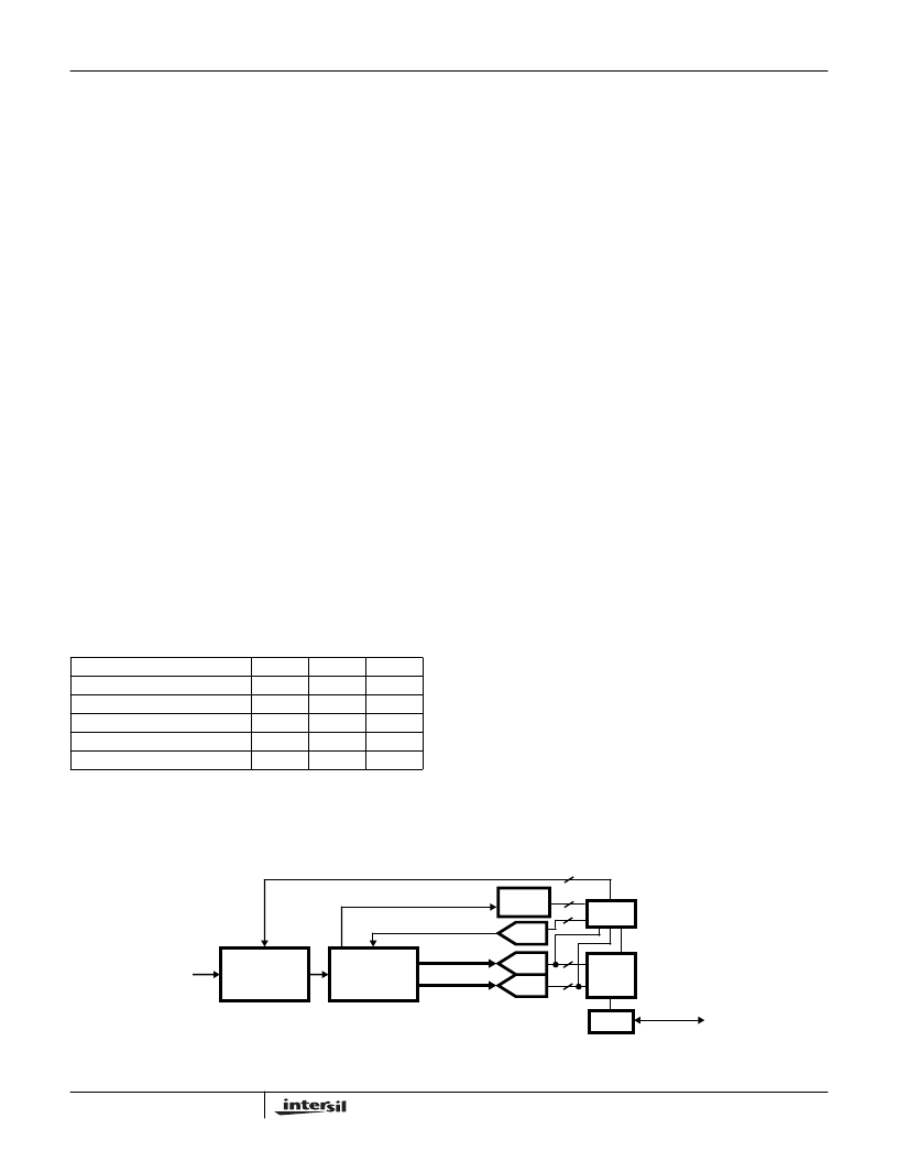
AGC Circuit
The AGC circuit is designed to optimize A/D performance for
the I and Q inputs by maintaining the proper headroom on
the 6-bit converters. There are two gain stages being
controlled. At RF, the gain control is a 30dB step in gain from
turning off the LNA. This RF gain control optimizes the
receiver dynamic range when the signal level is high and
maintains the noise figure of the receiver when it is needed
most. At IF the gain control is linear and covers the bulk of
the gain control range of the receiver.
The AGC sensing mechanism uses a combination of the
I and Q A/D converters and the detected signal level in the IF
to determine the gain settings. The A/D outputs are
monitored in the HFA3861B for the desired nominal level.
When it is reached, by adjusting the receiver gain, the gain
control is locked for the remainder of the packet.
RX_AGC_IN Interface
The signal level in the IF stage is monitored to determine
when to impose the up to 30dB gain reduction in the RF
stage. This maximizes the dynamic range of the receiver by
keeping the RF stages out of saturation at high signal levels.
When the IF circuits’ sensor output reaches 0.5V, the
HFA3861B comparator switches in the 30dB pad and
compensates the IF AGC and RSSI measures.
TX I/Q DAC Interface
The transmit section outputs balanced differential analog
signals from the transmit DACs to the HFA3783. These are
DC coupled and digitally filtered.
Test Port
The HFA3861B provides the capability to access a number of
internal signals and/or data through the Test port, pins TEST
7:0. The test port is programmable through configuration
register (CR 34). Any signal on the test port can also be read
from configuration register (CR50) via the serial control port.
Additionally, the transmit DACs can be configured to show
signals in the receiver via CR 14. This allows visibility to
analog like signals that would normally be very difficult to
capture.
TABLE 1. I, Q, A/D SPECIFICATIONS
PARAMETER
MIN
0.90
-
-
5k
-
TYP
1.00
11MHz
2
-
22MHz
MAX
1.10
-
-
-
-
Full Scale Input Voltage (V
Input Bandwidth (-0.5dB)
Input Capacitance (pF)
Input Impedance (DC)
f
S
(Sampling Frequency)
P-P
)
FIGURE 6. AGC CIRCUIT
RX_RF_AGC
RX_IF_DET
THRESH.
DETECT
IF
DAC
I ADC
Q ADC
RX_Q
±
RX_I
±
RX_IF_AGC
HFA3683
HFA3783
HFA3861B
6
6
7
1
1
I/O
DEMOD
AGC
CTL
DATA I/O
HFA3861B
相关PDF资料 |
PDF描述 |
|---|---|
| HFA3925IA | null2.4GHz - 2.5GHz 250mW Power Amplifier |
| HFA3925IA96 | null2.4GHz - 2.5GHz 250mW Power Amplifier |
| HFA50PA60C | RxxP2xx Series - Econoline Unregulated DC-DC Converters; Input Voltage (Vdc): 05V; Output Voltage (Vdc): 15V; Power: 2W; EN 60950 certified, rated for 250VAC; UL-60950-1 / CSA C22.2 certified; 5.2kVDC Isolation for 1 Minute; Optional Continuous Short Circuit Protected; Wide Operating Temperature Range atfull 2 Watts Load, ?40??C to +85??C; Twin Chamber Transformer System; UL94V-0 Package Material; Efficiency to 80% |
| HFB50PA60C | Ultrafast, Soft Recovery Diode |
| HFA5250 | 500MHz, Ultra High Speed Monolithic Pin Driver |
相关代理商/技术参数 |
参数描述 |
|---|---|
| HFA3861IV | 制造商:INTERSIL 制造商全称:Intersil Corporation 功能描述:Direct Sequence Spread Spectrum Baseband Processor |
| HFA3861IV96 | 制造商:INTERSIL 制造商全称:Intersil Corporation 功能描述:Direct Sequence Spread Spectrum Baseband Processor |
| HFA3863 | 制造商:INTERSIL 制造商全称:Intersil Corporation 功能描述:Direct Sequence Spread Spectrum Baseband Processor |
| HFA3863IN | 制造商:INTERSIL 制造商全称:Intersil Corporation 功能描述:Direct Sequence Spread Spectrum Baseband Processor |
| HFA3863IN96 | 制造商:INTERSIL 制造商全称:Intersil Corporation 功能描述:Direct Sequence Spread Spectrum Baseband Processor |
发布紧急采购,3分钟左右您将得到回复。