- 您现在的位置:买卖IC网 > PDF目录385380 > HI5741 (Intersil Corporation) 14-Bit, 100MSPS, High Speed D/A Converter(14位,100MHz,高速D/A转换器) PDF资料下载
参数资料
| 型号: | HI5741 |
| 厂商: | Intersil Corporation |
| 英文描述: | 14-Bit, 100MSPS, High Speed D/A Converter(14位,100MHz,高速D/A转换器) |
| 中文描述: | 14位,100MSPS时,高速D / A转换(14位,100MHz的,高速的D / A转换器) |
| 文件页数: | 10/13页 |
| 文件大小: | 354K |
| 代理商: | HI5741 |
10
FN4071.12
September 20, 2006
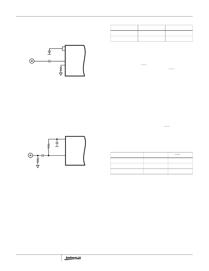
Multiplying Capability
The HI5741 can operate in two different multiplying
configurations. For frequencies from DC to 100kHz, a signal
of up to 0.6V
P-P
can be applied directly to the REF OUT pin
as shown in Figure 22.
The signal must have a DC value such that the peak
negative voltage equals -1.25V. Alternately, a capacitor can
be placed in series with REF OUT if a DC multiplying is not
required. The lower input bandwidth can be calculated using
the following formula:
For multiplying frequencies above 100kHz, the CTRL IN pin
can be driven directly as seen in Figure 23.
The nominal input/output relationship is defined as:
In order to prevent the full scale output current from
exceeding 20.48mA, the R
SET
resistor must be adjusted
according to the following equation:
The circuit in Figure 23 can be tuned to adjust the lower
cutoff frequency by adjusting capacitor values. Table 1
illustrates the relationship.
Also, the input signal must be limited to 1V
P-P
to avoid
distortion in the DAC output current caused by excessive
modulation of the internal current sources.
Outputs
The outputs I
OUT
and I
OUT
are complementary current
outputs. Current is steered to either I
OUT
or I
OUT
in proportion
to the digital input code. The sum of the two currents is always
equal to the full scale current minus one LSB. The current
output can be converted to a voltage by using a load resistor.
Both current outputs should have the same load resistor (64
typically). By using a 64
load on the output, a 50
effective
output resistance (R
OUT
) is achieved due to the 227
(
±
15%)
parallel resistance seen looking back into the output. This is the
nominal value of the R2R ladder of the DAC. The 50
output is
needed for matching the output with a 50
line. The load
resistor should be chosen so that the effective output resistance
(R
OUT
) matches the line resistance. The output voltage is:
V
OUT
= I
OUT
x R
OUT
.
I
OUT
is defined in the reference section. I
OUT
is not trimmed to
14 bits, so it is not recommended that it be used in conjunction
with I
OUT
in a differential-to-single-ended application. The
compliance range of the output is from -1.25V to 0V, with a
1V
P-P
voltage swing allowed within this range.
Settling Time
The settling time of the HI5741 is measured as the time it
takes for the output of the DAC to settle to within a ±defined
error band of its final value during a
1
/
16
th (code 0000... to
0001 0000.... or 1111... to 1110 1111...) scale transition. In
defining settling time specifications for the HI5741, two levels
of accuracy are considered. The accuracy levels defined for
the HI5741 are 12 (or 0.024%) and 13 (0.012%) bits.
Glitch
The output glitch of the HI5741 is measured by summing the
area under the switching transients after an update of the
DAC. Glitch is caused by the time skew between bits of the
incoming digital data. Typically, the switching time of digital
inputs are asymmetrical meaning that the turn off time is
faster than the turn on time (TTL designs). Unequal delay
paths through the device can also cause one current source
FIGURE 22. LOW FREQUENCY MULTIPLYING BANDWIDTH
CIRCUIT
REF OUT
RSET
HI5741
C
IN
(OPTIONAL)
0.01
μ
F
V
IN
CTRL OUT
CTRL IN
AV
EE
C
IN
2
(
)
1400
(
)
f
IN
(
)
-------------------------------------------
=
FIGURE 23. HIGH FREQUENCY MULTIPLYING BANDWIDTH
CIRCUIT
HI5741
CTRL IN
V
IN
CTRL OUT
AV
EE
200
C
2
C
1
50
I
OUT
V
80
-------------
=
R
SET
16V
I
OUT
Full scale
(
)
80
)
-----------------------------
–
-----------------------------------------------------------------------------------------
=
TABLE 1. CAPACITOR SELECTION
f
IN
C
1
C
2
100kHz
0.01
μ
F
1
μ
F
>1MHz
0.001
μ
F
0.1
μ
F
TABLE 2. INPUT CODING vs CURRENT OUTPUT
INPUT CODE (D13-D0)
I
OUT
(mA)
I
OUT
(mA)
11 1111 1111 1111
-20.48
0
10 0000 0000 0000
-10.24
-10.24
00 0000 0000 0000
0
-20.48
HI5741
相关PDF资料 |
PDF描述 |
|---|---|
| HI5746 | 10-Bit, 40 MSPS A/D Converter(10位、采样速率为40MSPS的A/D转换器) |
| HI5762EVAL2 | Dual 10-Bit, 60MSPS A/D Converter with Internal Voltage Reference |
| HI5780JCQ | 10-Bit, 80 MSPS, High Speed, Low Power D/A Converter |
| HI5780 | 10-Bit, 80 MSPS, High Speed, Low Power D/A Converter |
| HI5780-EV | 10-Bit, 80 MSPS, High Speed, Low Power D/A Converter |
相关代理商/技术参数 |
参数描述 |
|---|---|
| HI5741_06 | 制造商:INTERSIL 制造商全称:Intersil Corporation 功能描述:14-Bit, 100MSPS, High Speed D/A Converter |
| HI5741BIB | 功能描述:IC DAC 14-BIT 100MSPS 28-SOIC RoHS:否 类别:集成电路 (IC) >> 数据采集 - 数模转换器 系列:- 标准包装:2,400 系列:- 设置时间:- 位数:18 数据接口:串行 转换器数目:3 电压电源:模拟和数字 功率耗散(最大):- 工作温度:-40°C ~ 85°C 安装类型:表面贴装 封装/外壳:36-TFBGA 供应商设备封装:36-TFBGA 包装:带卷 (TR) 输出数目和类型:* 采样率(每秒):* |
| HI5741BIBS2503 | 制造商:Rochester Electronics LLC 功能描述:- Bulk |
| HI5741BIB-T | 功能描述:DAC 14BIT 100MHZ 5.2V 28-SOIC RoHS:否 类别:集成电路 (IC) >> 数据采集 - 数模转换器 系列:- 标准包装:2,400 系列:- 设置时间:- 位数:18 数据接口:串行 转换器数目:3 电压电源:模拟和数字 功率耗散(最大):- 工作温度:-40°C ~ 85°C 安装类型:表面贴装 封装/外壳:36-TFBGA 供应商设备封装:36-TFBGA 包装:带卷 (TR) 输出数目和类型:* 采样率(每秒):* |
| HI5741BIBZ | 功能描述:数模转换器- DAC 28 INDTEMP D/A 14 BIT 100 MHZ -5 2V RoHS:否 制造商:Texas Instruments 转换器数量:1 DAC 输出端数量:1 转换速率:2 MSPs 分辨率:16 bit 接口类型:QSPI, SPI, Serial (3-Wire, Microwire) 稳定时间:1 us 最大工作温度:+ 85 C 安装风格:SMD/SMT 封装 / 箱体:SOIC-14 封装:Tube |
发布紧急采购,3分钟左右您将得到回复。