- 您现在的位置:买卖IC网 > PDF目录385380 > HI5741 (Intersil Corporation) 14-Bit, 100MSPS, High Speed D/A Converter(14位,100MHz,高速D/A转换器) PDF资料下载
参数资料
| 型号: | HI5741 |
| 厂商: | Intersil Corporation |
| 英文描述: | 14-Bit, 100MSPS, High Speed D/A Converter(14位,100MHz,高速D/A转换器) |
| 中文描述: | 14位,100MSPS时,高速D / A转换(14位,100MHz的,高速的D / A转换器) |
| 文件页数: | 9/13页 |
| 文件大小: | 354K |
| 代理商: | HI5741 |
9
FN4071.12
September 20, 2006
Detailed Description
The HI5741 is a 14-bit, current out D/A converter. The DAC
can convert at 100 MSPS and runs on +5V and -5.2V
supplies. The architecture is an R/2R and segmented
switching current cell arrangement to reduce glitch. Laser
trimming is employed to tune linearity to true 14-bit levels.
The HI5741 achieves its low power and high speed
performance from an advanced BiCMOS process. The
HI5741 consumes 650mW (typical) and has an improved
hold time of only 0.25ns (typical). The HI5741 is an excellent
converter for use in communications applications and high
performance video systems.
Digital Inputs
The HI5741 is a TTL/CMOS compatible D/A. Data is latched
by a Master register. Once latched, data inputs D0 (LSB)
through D13 (MSB) are internally translated from TTL to ECL.
The internal latch and switching current source controls are
implemented in ECL technology to maintain high switching
speeds and low noise characteristics.
Decoder/Driver
The architecture employs a split R/2R ladder and segmented
current source arrangement. Bits D0 (LSB) through D9 directly
drive a typical R/2R network to create the binary weighted
current sources. Bits D10 through D13 (MSB) pass through a
“thermometer” decoder that converts the incoming data into 15
individual segmented current source enables. This split
architecture helps to improve glitch, thus resulting in a
more constant glitch characteristic across the entire output
transfer function.
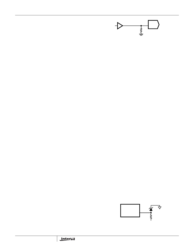
Clocks and Termination
The internal 14-bit register is updated on the rising edge of the
clock. Since the HI5741 clock rate can run to 100 MSPS, to
minimize reflections and clock noise into the part, proper
termination should be used. In PCB layout clock runs should
be kept short and have a minimum of loads. To guarantee
consistent results from board to board, controlled impedance
PCBs should be used with a characteristic line impedance Z
O
of 50
.
To terminate the clock line, a shunt terminator to ground is
the most effective type at a 100 MSPS clock rate. A typical
value for termination can be determined by the equation:
R
T
for the termination resistor. For a controlled impedance board
with a Z
O
of 50
, the R
T
= 50
. Shunt termination is best
used at the receiving end of the transmission line or as close
to the HI5741 CLK pin as possible.
Rise and Fall times and propagation delay of the line will be
affected by the shunt terminator. The terminator should be
connected to DGND.
Noise Reduction
To reduce power supply noise, separate analog and digital
power supplies should be used with 0.1
μ
F and 0.01
μ
F
ceramic capacitors placed as close to the body of the
HI5741 as possible on the analog (AV
EE
) and digital (DV
EE
)
supplies. The analog and digital ground returns should be
connected together back at the device to ensure proper
operation on power up. The V
CC
power pin should also be
decoupled with a 0.1
μ
F capacitor.
Reduction of digital noise (caused by high slew rates on the bit
inputs to the HI5741) can be accomplished through the use of
series termination resistors. The use of serial resistors, which
combine with the input capacitance of the HI5741 to induce a
low pass filter characteristic, keeps the noise generated by high
slew rate digital signals from corrupting the high accuracy
analog data. Refer to Application Note AN9619 “Optimizing
setup conditions for high accuracy measurements of the
HI5741” for further details on selecting the proper value of
series termination to meet application specific needs.
Reference
The internal reference of the HI5741 is a -1.23V (typical)
bandgap voltage reference with 50
μ
V/°C of temperature drift
(typical). The internal reference is connected to the Control
Amplifier which in turn drives the segmented current cells.
Reference Out (REF OUT) is internally connected to the
Control Amplifier. The Control Amplifier Output (CTRL OUT)
should be used to drive the Control Amplifier Input (CTRL IN)
and a 0.1
μ
F capacitor to analog V
EE
. This improves settling
time by providing an AC ground at the current source base
node. The Full Scale Output Current is controlled by the REF
OUT pin and the set resistor (R
SET
). The ratio is:
I
OUT
(Full Scale) = (V
REF OUT
/R
SET
) x 16.
The internal reference (REF OUT) can be overdriven with a
more precise external reference to provide better
performance over temperature. Figure 21 illustrates a typical
external reference configuration.
Z
O
=
R
T
= 50
HI5741
DAC
CLK
Z
O
= 50
FIGURE 20. HI5741 CLOCK LINE TERMINATION
FIGURE 21. EXTERNAL REFERENCE CONFIGURATION
(26) REF OUT
HI5741
R
-5.2V
-1.25V
HI5741
相关PDF资料 |
PDF描述 |
|---|---|
| HI5746 | 10-Bit, 40 MSPS A/D Converter(10位、采样速率为40MSPS的A/D转换器) |
| HI5762EVAL2 | Dual 10-Bit, 60MSPS A/D Converter with Internal Voltage Reference |
| HI5780JCQ | 10-Bit, 80 MSPS, High Speed, Low Power D/A Converter |
| HI5780 | 10-Bit, 80 MSPS, High Speed, Low Power D/A Converter |
| HI5780-EV | 10-Bit, 80 MSPS, High Speed, Low Power D/A Converter |
相关代理商/技术参数 |
参数描述 |
|---|---|
| HI5741_06 | 制造商:INTERSIL 制造商全称:Intersil Corporation 功能描述:14-Bit, 100MSPS, High Speed D/A Converter |
| HI5741BIB | 功能描述:IC DAC 14-BIT 100MSPS 28-SOIC RoHS:否 类别:集成电路 (IC) >> 数据采集 - 数模转换器 系列:- 标准包装:2,400 系列:- 设置时间:- 位数:18 数据接口:串行 转换器数目:3 电压电源:模拟和数字 功率耗散(最大):- 工作温度:-40°C ~ 85°C 安装类型:表面贴装 封装/外壳:36-TFBGA 供应商设备封装:36-TFBGA 包装:带卷 (TR) 输出数目和类型:* 采样率(每秒):* |
| HI5741BIBS2503 | 制造商:Rochester Electronics LLC 功能描述:- Bulk |
| HI5741BIB-T | 功能描述:DAC 14BIT 100MHZ 5.2V 28-SOIC RoHS:否 类别:集成电路 (IC) >> 数据采集 - 数模转换器 系列:- 标准包装:2,400 系列:- 设置时间:- 位数:18 数据接口:串行 转换器数目:3 电压电源:模拟和数字 功率耗散(最大):- 工作温度:-40°C ~ 85°C 安装类型:表面贴装 封装/外壳:36-TFBGA 供应商设备封装:36-TFBGA 包装:带卷 (TR) 输出数目和类型:* 采样率(每秒):* |
| HI5741BIBZ | 功能描述:数模转换器- DAC 28 INDTEMP D/A 14 BIT 100 MHZ -5 2V RoHS:否 制造商:Texas Instruments 转换器数量:1 DAC 输出端数量:1 转换速率:2 MSPs 分辨率:16 bit 接口类型:QSPI, SPI, Serial (3-Wire, Microwire) 稳定时间:1 us 最大工作温度:+ 85 C 安装风格:SMD/SMT 封装 / 箱体:SOIC-14 封装:Tube |
发布紧急采购,3分钟左右您将得到回复。