- 您现在的位置:买卖IC网 > PDF目录385380 > HI5741 (Intersil Corporation) 14-Bit, 100MSPS, High Speed D/A Converter(14位,100MHz,高速D/A转换器) PDF资料下载
参数资料
| 型号: | HI5741 |
| 厂商: | Intersil Corporation |
| 英文描述: | 14-Bit, 100MSPS, High Speed D/A Converter(14位,100MHz,高速D/A转换器) |
| 中文描述: | 14位,100MSPS时,高速D / A转换(14位,100MHz的,高速的D / A转换器) |
| 文件页数: | 3/13页 |
| 文件大小: | 354K |
| 代理商: | HI5741 |
3
FN4071.12
September 20, 2006
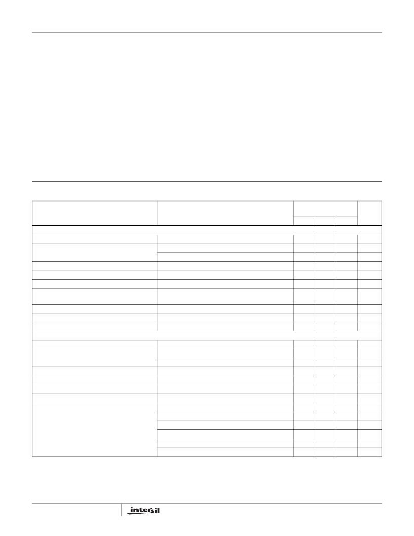
Absolute Maximum ratings
T
A
= +25°C
Digital Supply Voltage V
CC
to DGND . . . . . . . . . . . . . . . . . . . +5.5V
Negative Digital Supply Voltage DV
EE
to DGND . . . . . . . . . . -5.5V
Negative Analog Supply Voltage AV
EE
to AGND, ARTN . . . . -5.5V
Digital Input Voltages (D13-D0, CLK) to DGND. . . . . DV
CC
to -0.5V
Internal Reference Output Current. . . . . . . . . . . . . . . . . . . .
±
2.5mA
Voltage from CTRL AMP IN to AV
EE
. . . . . . . . . . . . . . . . 2.5V to 0V
Control Amplifier Output Current . . . . . . . . . . . . . . . . . . . . .
±
2.5mA
Reference Input Voltage Range. . . . . . . . . . . . . . . . . -3.7V to AV
EE
Analog Output Current (I
OUT
) . . . . . . . . . . . . . . . . . . . . . . . . . 30mA
Thermal Information
Operating Conditions
Temperature Range. . . . . . . . . . . . . . . . . . . . . . . . . .-40°C to +85°C
Thermal Resistance (Typical, Note 1)
SOIC Package . . . . . . . . . . . . . . . . . . . . . . . . . . .
Maximum Junction Temperature
HI5741BIx . . . . . . . . . . . . . . . . . . . . . . . . . . . . . . . . . . . . .+150°C
Maximum Storage Temperature Range . . . . . . . . .-65°C to +150°C
Maximum Lead Temperature (Soldering 10s). . . . . . . . . . . .+300°C
(SOIC - Lead Tips Only)
θ
JA
(°C/W)
70
CAUTION: Stresses above those listed in “Absolute Maximum Ratings” may cause permanent damage to the device. This is a stress only rating and operation of the
device at these or any other conditions above those indicated in the operational sections of this specification is not implied.
NOTE:
1.
θ
JA
is measured with the component mounted on a low effective thermal conductivity test board in free air. See Tech Brief TB379 for details.
Electrical Specifications
AV
EE
, DV
EE
= -4.94V to -5.46V, V
CC
= +4.75 to +5.25V, V
REF
= Internal,
T
A
= +25°C
PARAMETER
TEST CONDITIONS
HI5741BI
T
A
= -40°C TO +85°C
MIN
TYP
UNITS
MAX
SYSTEM PERFORMANCE
Resolution
14
-
-
Bits
Integral Linearity Error, INL
(Note 5)
“Best Fit Straight Line”, T
A
= +25°C
“Best Fit Straight Line”, T
A
= -40°C to +85°C
(Note 5) T
A
= +25°C
(Note 5)
-1.5
±1.0
1.5
LSB
-1.75
-
1.75
LSB
Differential Linearity Error, DNL
-1.0
±0.5
1.0
LSB
μ
A
Offset Error, I
OS
Full Scale Gain Error, FSE
-
8
75
(Notes 3, 5)
-
3.2
10
%
Full Scale Gain Drift
With Internal Reference
-
±150
-
ppm
FSR/°C
μ
A/°C
Offset Drift Coefficient
(Note 4)
-
-
0.05
Full Scale Output Current, I
FS
Output Voltage Compliance Range
-
-20.48
-
mA
(Note 4)
-1.25
-
0
V
DYNAMIC CHARACTERISTICS
Throughput Rate
(Note 4)
R
L
= 64
(Note 4) - Settling to 0.024%
R
L
= 64
(Note 4) - Settling to 0.012%
R
L
= 64
(Note 4)
R
L
= 64
,
DAC Operating in Latched Mode (Note 4)
R
L
= 64
,
DAC Operating in Latched Mode (Note 4)
R
L
= 64
,
DAC Operating in Latched Mode (Note 4)
f
CLK
= 10 MSPS, f
OUT
= 1.23MHz, 2MHz Span
f
CLK
= 20 MSPS, f
OUT
= 5.055MHz, 2MHz Span
f
CLK
= 40 MSPS, f
OUT
= 16MHz, 10MHz Span
f
CLK
= 50 MSPS, f
OUT
= 10.1MHz, 2MHz Span
f
CLK
= 80 MSPS, f
OUT
= 5.1MHz, 2MHz Span
f
CLK
= 100 MSPS, f
OUT
= 10.1MHz, 2MHz Span
100
-
-
MSPS
Output Voltage Settling Time
(
1
/
16
th Scale Step Across Segment)
-
11
-
ns
-
20
-
ns
Singlet Glitch Area, GE (Peak)
-
1
-
pVs
V/
μ
s
Output Slew Rate
-
1,000
-
Output Rise Time
-
675
-
ps
Output Fall Time
-
470
-
ps
Spurious Free Dynamic Range within a Window
(Note 4)
-
87
-
dBc
-
77
-
dBc
-
75
-
dBc
-
80
-
dBc
-
78
-
dBc
-
79
-
dBc
HI5741
相关PDF资料 |
PDF描述 |
|---|---|
| HI5746 | 10-Bit, 40 MSPS A/D Converter(10位、采样速率为40MSPS的A/D转换器) |
| HI5762EVAL2 | Dual 10-Bit, 60MSPS A/D Converter with Internal Voltage Reference |
| HI5780JCQ | 10-Bit, 80 MSPS, High Speed, Low Power D/A Converter |
| HI5780 | 10-Bit, 80 MSPS, High Speed, Low Power D/A Converter |
| HI5780-EV | 10-Bit, 80 MSPS, High Speed, Low Power D/A Converter |
相关代理商/技术参数 |
参数描述 |
|---|---|
| HI5741_06 | 制造商:INTERSIL 制造商全称:Intersil Corporation 功能描述:14-Bit, 100MSPS, High Speed D/A Converter |
| HI5741BIB | 功能描述:IC DAC 14-BIT 100MSPS 28-SOIC RoHS:否 类别:集成电路 (IC) >> 数据采集 - 数模转换器 系列:- 标准包装:2,400 系列:- 设置时间:- 位数:18 数据接口:串行 转换器数目:3 电压电源:模拟和数字 功率耗散(最大):- 工作温度:-40°C ~ 85°C 安装类型:表面贴装 封装/外壳:36-TFBGA 供应商设备封装:36-TFBGA 包装:带卷 (TR) 输出数目和类型:* 采样率(每秒):* |
| HI5741BIBS2503 | 制造商:Rochester Electronics LLC 功能描述:- Bulk |
| HI5741BIB-T | 功能描述:DAC 14BIT 100MHZ 5.2V 28-SOIC RoHS:否 类别:集成电路 (IC) >> 数据采集 - 数模转换器 系列:- 标准包装:2,400 系列:- 设置时间:- 位数:18 数据接口:串行 转换器数目:3 电压电源:模拟和数字 功率耗散(最大):- 工作温度:-40°C ~ 85°C 安装类型:表面贴装 封装/外壳:36-TFBGA 供应商设备封装:36-TFBGA 包装:带卷 (TR) 输出数目和类型:* 采样率(每秒):* |
| HI5741BIBZ | 功能描述:数模转换器- DAC 28 INDTEMP D/A 14 BIT 100 MHZ -5 2V RoHS:否 制造商:Texas Instruments 转换器数量:1 DAC 输出端数量:1 转换速率:2 MSPs 分辨率:16 bit 接口类型:QSPI, SPI, Serial (3-Wire, Microwire) 稳定时间:1 us 最大工作温度:+ 85 C 安装风格:SMD/SMT 封装 / 箱体:SOIC-14 封装:Tube |
发布紧急采购,3分钟左右您将得到回复。