参数资料
| 型号: | HI5767/4CB-T |
| 厂商: | Intersil |
| 文件页数: | 3/15页 |
| 文件大小: | 0K |
| 描述: | CONV A/D 10BIT 40MSPS 28-SOIC |
| 标准包装: | 1,000 |
| 位数: | 10 |
| 采样率(每秒): | 40M |
| 数据接口: | 并联 |
| 转换器数目: | 8 |
| 功率耗散(最大): | 310mW |
| 电压电源: | 模拟和数字 |
| 工作温度: | 0°C ~ 70°C |
| 安装类型: | 表面贴装 |
| 封装/外壳: | 28-SOIC(0.295",7.50mm 宽) |
| 供应商设备封装: | 28-SOIC W |
| 包装: | 带卷 (TR) |
| 输入数目和类型: | 2 个单端,单极;1 个差分,双极 |
11
Detailed Description
Theory of Operation
The HI5767 is a 10-bit fully differential sampling pipeline A/D
converter with digital error correction logic. Figure 16 depicts
the circuit for the front end differential-in-differential-out sample-
and-hold (S/H). The switches are controlled by an internal
sampling clock which is a non-overlapping two phase signal
, Φ
1
and
Φ
2, derived from the master sampling clock. During the
sampling phase,
Φ
1, the input signal is applied to the sampling
capacitors, CS. At the same time the holding capacitors, CH,
are discharged to analog ground. At the falling edge of
Φ
1 the
input signal is sampled on the bottom plates of the sampling
capacitors. In the next clock phase,
Φ
2, the two bottom plates
of the sampling capacitors are connected together and the
holding capacitors are switched to the op-amp output nodes.
The charge then redistributes between CS and CH completing
one sample-and-hold cycle. The front end sample-and-hold
output is a fully-differential, sampled-data representation of the
analog input. The circuit not only performs the sample-and-hold
function but will also convert a single-ended input to a fully-
differential output for the converter core. During the sampling
phase, the VIN pins see only the on-resistance of a switch and
CS. The relatively small values of these components result in a
typical full power input bandwidth of 250MHz for the converter.
As illustrated in the functional block diagram and the timing
diagram in Figure 1, eight identical pipeline subconverter
stages, each containing a two-bit flash converter and a two-
bit multiplying digital-to-analog converter, follow the S/H
circuit with the ninth stage being a two bit flash converter.
Each converter stage in the pipeline will be sampling in one
phase and amplifying in the other clock phase. Each
individual subconverter clock signal is offset by 180 degrees
from the previous stage clock signal resulting in alternate
stages in the pipeline performing the same operation.
The output of each of the eight identical two-bit subconverter
stages is a two-bit digital word containing a supplementary bit
to be used by the digital error correction logic. The output of
each subconverter stage is input to a digital delay line which is
controlled by the internal sampling clock. The function of the
digital delay line is to time align the digital outputs of the eight
identical two-bit subconverter stages with the corresponding
output of the ninth stage flash converter before applying the
eighteen bit result to the digital error correction logic. The
digital error correction logic uses the supplementary bits to
correct any error that may exist before generating the final ten
bit digital data output of the converter.
Because of the pipeline nature of this converter, the digital data
representing an analog input sample is output to the digital data
bus on the 7th cycle of the clock after the analog sample is
taken. This time delay is specified as the data latency. After the
data latency time, the digital data representing each
succeeding analog sample is output during the following clock
cycle. The digital output data is synchronized to the external
sampling clock by a double buffered latching technique. The
digital output data is available in two’s complement or offset
binary format depending on the state of the Data Format Select
(DFS) control input (see Table 1, A/D Code Table).
Internal Reference Voltage Output, VREFOUT
The HI5767 is equipped with an internal reference voltage
generator, therefore, no external reference voltage is
required. VREFOUT must be connected to VREFIN when using
the internal reference voltage.
An internal band-gap reference voltage followed by an
amplifier/buffer generates the precision +2.5V reference
voltage used by the converter. A 4:1 array of substrate
PNPs generates the “delta-VBE” and a two-stage op-amp
closes the loop to create an internal +1.25V band-gap
reference voltage. This voltage is then amplified by a
wideband uncompensated operational amplifier connected
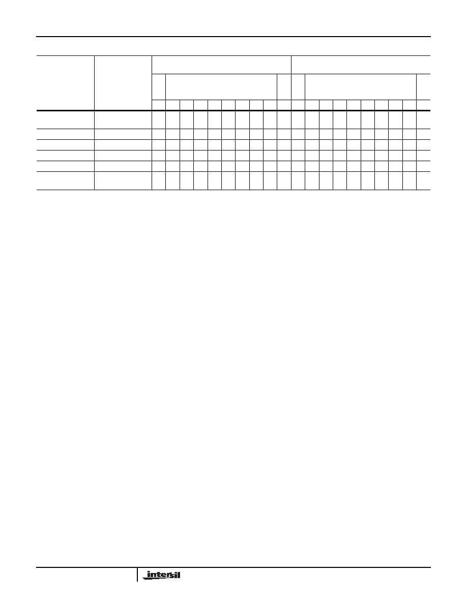
TABLE 1. A/D CODE TABLE
CODE CENTER
DESCRIPTION
DIFFERENTIAL
INPUT VOLTAGE
(VIN+ - VIN-)
OFFSET BINARY OUTPUT CODE
(DFS LOW)
TWO’S COMPLEMENT OUTPUT CODE
(DFS HIGH)
M
S
B
L
S
B
M
S
B
L
S
B
D9
D8
D7
D6
D5
D4
D3
D2
D1
D0
D9
D8
D7
D6
D5
D4
D3
D2
D1
D0
+Full Scale (+FS) -
1/
4 LSB
0.499756V
1
0
1
+FS
- 11/4 LSB
0.498779V
1
0
1
0
+3/4 LSB
732.422
V
1
0
-1/4 LSB
-244.141
V
0
1
-FS + 13/4 LSB
-0.498291V
0
1
0
1
-Full Scale (-FS) +
3/
4 LSB
-0.499268V
0
1
0
NOTE:
4. The voltages listed above represent the ideal center of each output code shown with VREFIN = +2.5V.
HI5767
相关PDF资料 |
PDF描述 |
|---|---|
| MAX4952CTO+ | IC RE-DRIVER 4CH SAS/SATA 42TQFN |
| V375C12M150BL2 | CONVERTER MOD DC/DC 12V 150W |
| VI-243-MX-F2 | CONVERTER MOD DC/DC 24V 75W |
| HI5767/4CB | CONV A/D 10BIT 40MSPS 28-SOIC |
| VE-26D-IU-F1 | CONVERTER MOD DC/DC 85V 200W |
相关代理商/技术参数 |
参数描述 |
|---|---|
| HI5767EVAL1 | 功能描述:数据转换 IC 开发工具 HI5767 LW FREQUENCY EVALUATION PLATFORM RoHS:否 制造商:Texas Instruments 产品:Demonstration Kits 类型:ADC 工具用于评估:ADS130E08 接口类型:SPI 工作电源电压:- 6 V to + 6 V |
| HI5767EVAL2 | 功能描述:数据转换 IC 开发工具 HI5767 HI FREQUENCY EVALUATION PLATFORM RoHS:否 制造商:Texas Instruments 产品:Demonstration Kits 类型:ADC 工具用于评估:ADS130E08 接口类型:SPI 工作电源电压:- 6 V to + 6 V |
| HI5780 | 制造商:INTERSIL 制造商全称:Intersil Corporation 功能描述:10-Bit, 80 MSPS, High Speed, Low Power D/A Converter |
| HI5780-EV | 制造商:INTERSIL 制造商全称:Intersil Corporation 功能描述:10-Bit, 80 MSPS, High Speed, Low Power D/A Converter |
| HI5780JCQ | 制造商:Rochester Electronics LLC 功能描述:32 PQFP COMTEMP VIDEO D/A 10BIT 80MHZ - Bulk 制造商:Harris Corporation 功能描述: |
发布紧急采购,3分钟左右您将得到回复。